AD9834
TABLE OF CONTENTS
Features .............................................................................................. 1
Control Register ......................................................................... 18
Frequency and Phase Registers ................................................ 20
Writing to a Frequency Register............................................... 21
Writing to a Phase Register....................................................... 21
RESET Function......................................................................... 21
SLEEP Function.......................................................................... 21
SIGN BIT OUT Pin.................................................................... 22
The IOUT and IOUTB Pins...................................................... 22
Applications Information.............................................................. 23
Grounding and Layout .................................................................. 26
Interfacing to Microprocessors..................................................... 27
AD9834 to ADSP-21xx Interface ............................................. 27
AD9834 to 68HC11/68L11 Interface....................................... 27
AD9834 to 80C51/80L51 Interface.......................................... 28
AD9834 to DSP56002 Interface ............................................... 28
Evaluation Board ............................................................................ 29
System Development Platform................................................. 29
AD9834 to SPORT Interface..................................................... 29
XO vs. External Clock................................................................ 29
Power Supply............................................................................... 29
Evaluation Board Schematics ................................................... 30
Evaluation Board Layout........................................................... 32
Outline Dimensions....................................................................... 35
Ordering Guide .......................................................................... 35
Applications....................................................................................... 1
General Description......................................................................... 1
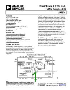
Functional Block Diagram .............................................................. 1
Revision History ............................................................................... 3
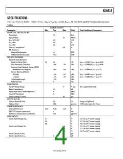
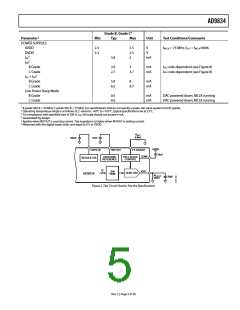
Specifications..................................................................................... 4
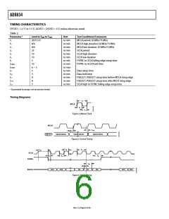
Timing Characteristics ................................................................ 6
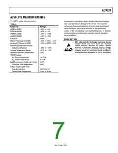
Absolute Maximum Ratings............................................................ 7
ESD Caution.................................................................................. 7
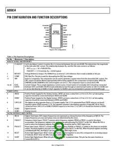
Pin Configuration and Function Descriptions............................. 8
Typical Performance Characteristics ........................................... 10
Terminology .................................................................................... 14
Theory of Operation ...................................................................... 15
Circuit Description......................................................................... 16
Numerically Controlled Oscillator Plus Phase Modulator... 16
SIN ROM..................................................................................... 16
Digital-to-Analog Converter (DAC) ....................................... 16
Comparator ................................................................................. 16
Regulator...................................................................................... 17
Output Voltage Compliance...................................................... 17
Functional Description.................................................................. 18
Serial Interface ............................................................................ 18
Powering Up the AD9834 ......................................................... 18
Latency......................................................................................... 18
Rev. C | Page 2 of 36

 ADI [ ADI ]