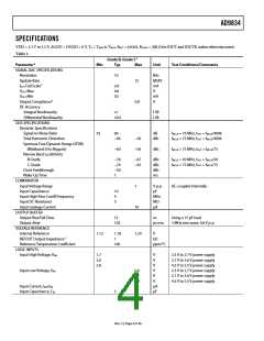
AD9834
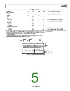
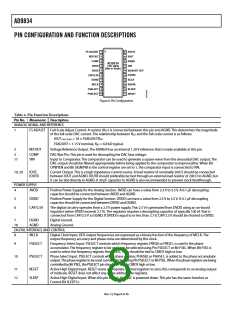
PIN CONFIGURATION AND FUNCTION DESCRIPTIONS
1
2
20
19
18
17
16
15
14
13
12
11
FS ADJUST
REFOUT
COMP
IOUTB
IOUT
3
AGND
AD9834
4
AVDD
VIN
TOP VIEW
(Not to Scale)
5
DVDD
SIGN BIT OUT
FSYNC
SCLK
6
CAP/2.5V
DGND
7
8
MCLK
SDATA
SLEEP
RESET
9
FSELECT
PSELECT
10
Figure 6. Pin Configuration
Table 4. Pin Function Descriptions
Pin No. Mnemonic Description
ANALOG SIGNAL AND REFERENCE
1
FS ADJUST Full-Scale Adjust Control. A resistor (RSET) is connected between this pin and AGND. This determines the magnitude
of the full-scale DAC current. The relationship between RSET and the full-scale current is as follows:
IOUT FULL SCALE = 18 × FSADJUST/RSET
FSADJUST = 1.15 V nominal, RSET = 6.8 ꢀΩ typical.
2
REFOUT
COMP
VIN
Voltage Reference Output. The AD9834 has an internal 1.20 V reference that is made available at this pin.
DAC Bias Pin. This pin is used for decoupling the DAC bias voltage.
Input to Comparator. The comparator can be used to generate a square wave from the sinusoidal DAC output. The
DAC output should be filtered appropriately before being applied to the comparator to improve jitter. When Bit
OPBITEN and Bit SIGN/PIB in the control register are set to 1, the comparator input is connected to VIN.
3
17
19, 20
IOUT,
IOUTB
Current Output. This is a high impedance current source. A load resistor of nominally 200 Ω should be connected
between IOUT and AGND. IOUTB should preferably be tied through an external load resistor of 200 Ω to AGND, but
it can be tied directly to AGND. A 20 pF capacitor to AGND is also recommended to prevent clocꢀ feedthrough.
POWER SUPPLY
4
5
6
AVDD
Positive Power Supply for the Analog Section. AVDD can have a value from 2.3 V to 5.5 V. A 0.1 μF decoupling
capacitor should be connected between AVDD and AGND.
Positive Power Supply for the Digital Section. DVDD can have a value from 2.3 V to 5.5 V. A 0.1 μF decoupling
capacitor should be connected between DVDD and DGND.
The digital circuitry operates from a 2.5 V power supply. This 2.5 V is generated from DVDD using an on-board
regulator (when DVDD exceeds 2.7 V). The regulator requires a decoupling capacitor of typically 100 nF that is
connected from CAP/2.5 V to DGND. If DVDD is equal to or less than 2.7 V, CAP/2.5 V should be shorted to DVDD.
DVDD
CAP/2.5V
7
18
DGND
AGND
Digital Ground.
Analog Ground.
DIGITAL INTERFACE AND CONTROL
8
MCLK
Digital Clocꢀ Input. DDS output frequencies are expressed as a binary fraction of the frequency of MCLK. The
output frequency accuracy and phase noise are determined by this clocꢀ.
9
FSELECT
Frequency Select Input. FSELECT controls which frequency register, FREQ0 or FREQ1, is used in the phase
accumulator. The frequency register to be used can be selected using Pin FSELECT or Bit FSEL. When Bit FSEL is
used to select the frequency register, the FSELECT pin should be tied to CMOS high or low.
10
PSELECT
Phase Select Input. PSELECT controls which phase register, PHASE0 or PHASE1, is added to the phase accumulator
output. The phase register to be used can be selected using Pin PSELECT or Bit PSEL. When the phase registers are being
controlled by Bit PSEL, the PSELECT pin should be tied to CMOS high or low.
11
12
RESET
SLEEP
Active High Digital Input. RESET resets appropriate internal registers to zero; this corresponds to an analog output
of midscale. RESET does not affect any of the addressable registers.
Active High Digital Input. When this pin is high, the DAC is powered down. This pin has the same function as
Control Bit SLEEP12.
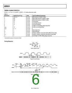
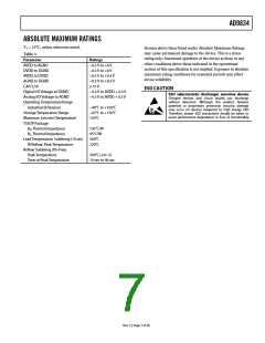
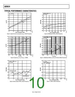
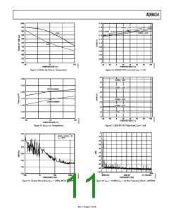
Rev. C | Page 8 of 36

 ADI [ ADI ]