20 mW Power, 2.3 V to 5.5 V,
75 MHz Complete DDS
AD9834
Capability for phase modulation and frequency modulation is
provided. The frequency registers are 28 bits; with a 75 MHz clock
rate, resolution of 0.28 Hz can be achieved. Similarly, with a 1 MHz
clock rate, the AD9834 can be tuned to 0.004 Hz resolution.
Frequency and phase modulation are affected by loading registers
through the serial interface and toggling the registers using
software or the FSELECT pin and PSELECT pin, respectively.
FEATURES
Narrow-band SFDR >72 dB
2.3 V to 5.5 V power supply
Output frequency up to 37.5 MHz
Sine output/triangular output
On-board comparator
3-wire SPI® interface
Extended temperature range: −40°C to +105°C
Power-down option
20 mW power consumption at 3 V
20-lead TSSOP
The AD9834 is written to using a 3-wire serial interface. This
serial interface operates at clock rates up to 40 MHz and is
compatible with DSP and microcontroller standards.
The device operates with a power supply from 2.3 V to 5.5 V.
The analog and digital sections are independent and can be run
from different power supplies, for example, AVDD can equal
5 V with DVDD equal to 3 V.
APPLICATIONS
Frequency stimulus/waveform generation
Frequency phase tuning and modulation
Low power RF/communications systems
Liquid and gas flow measurement
Sensory applications: proximity, motion, and defect
detection
The AD9834 has a power-down pin (SLEEP) that allows
external control of the power-down mode. Sections of the
device that are not being used can be powered down to
minimize the current consumption. For example, the DAC can
be powered down when a clock output is being generated.
Test and medical equipment
GENERAL DESCRIPTION
The part is available in a 20-lead TSSOP.
The AD9834 is a 75 MHz low power DDS device capable of
producing high performance sine and triangular outputs. It also
has an on-board comparator that allows a square wave to be
produced for clock generation. Consuming only 20 mW of power
at 3 V makes the AD9834 an ideal candidate for power-sensitive
applications.
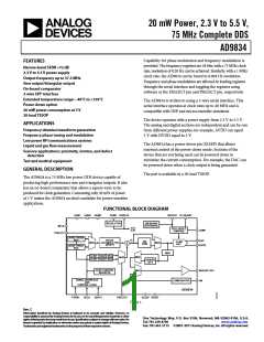
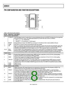
FUNCTIONAL BLOCK DIAGRAM
AVDD
AGND
DGND
DVDD CAP/2.5V
REFOUT FS ADJUST
REGULATOR
ON-BOARD
REFERENCE
MCLK
VCC
2.5V
FULL-SCALE
CONTROL
COMP
FSELECT
28-BIT FREQ0
REG
12
PHASE
ACCUMULATOR
(28-BIT)
IOUT
SIN
ROM
10-BIT
DAC
MUX
MUX
Σ
IOUTB
28-BIT FREQ1
REG
MSB
12-BIT PHASE0 REG
12-BIT PHASE1 REG
MUX
MUX
DIVIDED
BY 2
16-BIT CONTROL
REGISTER
MUX
SIGN BIT OUT
VIN
SERIAL INTERFACE
COMPARATOR
AND
CONTROL LOGIC
AD9834
FSYNC
SCLK
SDATA
PSELECT
SLEEP RESET
Figure 1.
Rev. C
Information furnished by Analog Devices is believed to be accurate and reliable. However, no
responsibility is assumed by Analog Devices for its use, nor for any infringements of patents or other
rights of third parties that may result from its use. Specifications subject to change without notice. No
license is granted by implication or otherwise under any patent or patent rights of Analog Devices.
Trademarks and registeredtrademarks arethe property of their respective owners.
One Technology Way, P.O. Box 9106, Norwood, MA 02062-9106, U.S.A.
Tel: 781.329.4700 www.analog.com
Fax: 781.461.3113 ©2003–2011 Analog Devices, Inc. All rights reserved.

 ADI [ ADI ]