AD9834
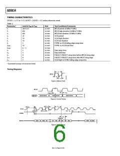
TIMING CHARACTERISTICS
DVDD = 2.3 V to 5.5 V, AGND = DGND = 0 V, unless otherwise noted.
Table 2.
Parameter1
Limit at TMIN to TMAX
Unit
Test Conditions/Comments
MCLK period: 50 MHz/75 MHz
MCLK high duration: 50 MHz/75 MHz
MCLK low duration: 50 MHz/75 MHz
SCLK period
SCLK high duration
SCLK low duration
FSYNC-to-SCLK falling edge setup time
FSYNC-to-SCLK hold time
t1
t2
t3
t4
t5
t6
t7
t8 MIN
t8 MAX
t9
t10
t11
t11A
t12
20/13.33
ns min
ns min
ns min
ns min
ns min
ns min
ns min
ns min
ns max
ns min
ns min
ns min
ns min
ns min
8/6
8/6
25
10
10
5
10
t4 − 5
5
3
8
8
5
Data setup time
Data hold time
FSELECT, PSELECT setup time before MCLK rising edge
FSELECT, PSELECT setup time after MCLK rising edge
SCLK high to FSYNC falling edge setup time
1 Guaranteed by design, not production tested.
Timing Diagrams
t1
MCLK
t2
t3
Figure 3. Master Clock
MCLK
t11A
t11
FSELECT,
PSELECT
VALID DATA
VALID DATA
VALID DATA
Figure 4. Control Timing
t5
t4
t12
SCLK
t7
t6
t8
FSYNC
t10
t9
SDATA
D15
D14
D2
D1
D0
D15
D14
Figure 5. Serial Timing
Rev. C | Page 6 of 36

 ADI [ ADI ]