AD9834
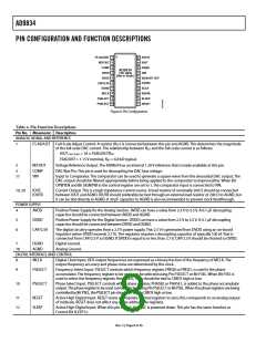
Pin No. Mnemonic Description
13
14
15
SDATA
SCLK
FSYNC
Serial Data Input. The 16-bit serial data-word is applied to this input.
Serial Clocꢀ Input. Data is clocꢀed into the AD9834 on each falling SCLK edge.
Active Low Control Input. This is the frame synchronization signal for the input data. When FSYNC is taꢀen low, the
internal logic is informed that a new word is being loaded into the device.
16
SIGN BIT
OUT
Logic Output. The comparator output is available on this pin or, alternatively, the MSB from the NCO can be output
on this pin. Setting Bit OPBITEN in the control register to 1 enables this output pin. Bit SIGN/PIB determines
whether the comparator output or the MSB from the NCO is output on the pin.
Rev. C | Page 9 of 36

 ADI [ ADI ]