ADV7180
MPU PORT DESCRIPTION
The ADV7180 supports a 2-wire (I2C-compatible) serial inter-
face. Two inputs, serial data (SDA) and serial clock (SCLK),
carry information between the ADV7180 and the system I2C
master controller. Each slave device is recognized by a unique
address. The ADV7180 I2C port allows the user to set up and
configure the decoder and to read back captured VBI data. The
ADV7180 has four possible slave addresses for both read and
write operations, depending on the logic level of the ALSB pin.
The four unique addresses are shown in Table 100. The ADV7180
ALSB pin controls Bit 1 of the slave address. By altering the ALSB,
it is possible to control two ADV7180s in an application without
having the conflict of using the same slave address. The LSB (Bit 0)
sets either a read or write operation. Logic 1 corresponds to a
read operation; Logic 0 corresponds to a write operation.
first byte means that the master writes information to the
peripheral. Logic 1 on the LSB of the first byte means that the
master reads information from the peripheral.
The ADV7180 acts as a standard slave device on the bus. The
data on the SDA pin is eight bits long, supporting the 7-bit
W
address plus the R/ bit. The device has 249 subaddresses to
enable access to the internal registers. It therefore interprets the
first byte as the device address and the second byte as the
starting subaddress. The subaddresses auto-increment, allowing
data to be written to or read from the starting subaddress. A
data transfer is always terminated by a stop condition. The user
can also access any unique subaddress register on a one-by-one
basis without updating all the registers.
Stop and start conditions can be detected at any stage during the
data transfer. If these conditions are asserted out of sequence with
normal read and write operations, they cause an immediate
jump to the idle condition. During a given SCLK high period,
the user should only issue one start condition, one stop condition,
or a single stop condition followed by a single start condition. If
an invalid subaddress is issued by the user, the ADV7180 does
not issue an acknowledge and returns to the idle condition.
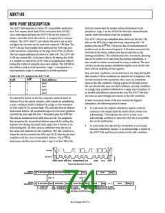
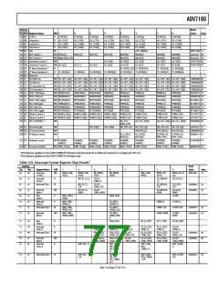
Table 100. I2C Address for ADV7180
R/W
ALSB
Slave Address
0x40
0x41
0x42
0x43
0
0
1
1
0
1
0
1
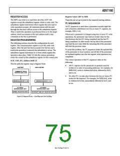
To control the device on the bus, a specific protocol must be
followed. First, the master initiates a data transfer by establishing
a start condition, which is defined by a high-to-low transition
on SDA while SCLK remains high. This indicates that an address/
data stream follows. All peripherals respond to the start condition
In auto-increment mode, if the user exceeds the highest
subaddress, the following action is taken:
•
In read mode, the highest subaddress register contents
continue to be output until the master device issues a no
acknowledge. This indicates the end of a read. A no
acknowledge condition is when the SDA line is not pulled
low on the ninth pulse.
and shift the next eight bits (the 7-bit address plus the R/ bit).
W
The bits are transferred from MSB down to LSB. The peripheral
that recognizes the transmitted address responds by pulling the
data line low during the ninth clock pulse; this is known as an
acknowledge bit. All other devices withdraw from the bus at
this point and maintain an idle condition. The idle condition is
where the device monitors the SDA and SCLK lines for the start
•
In write mode, the data for the invalid byte is not loaded
into any subaddress register. A no acknowledge is issued by
the ADV7180, and the part returns to the idle condition.
condition and the correct transmitted address. The R/ bit
W
determines the direction of the data. Logic 0 on the LSB of the
SDATA
SCLOCK
S
P
1–7
8
9
1–7
8
9
1–7
DATA
8
9
START ADDR R/W ACK SUBADDRESS ACK
ACK
STOP
Figure 48. Bus Data Transfer
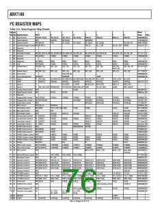
WRITE
S
S
SLAVE ADDR A(S) SUB ADDR
LSB = 0
A(S)
DATA
A(S)
DATA
A(M)
A(S) P
SEQUENCE
LSB = 1
READ
SEQUENCE
SLAVE ADDR A(S) SUB ADDR
A(S)
S
SLAVE ADDR A(S)
DATA
DATA
A(M) P
S = START BIT
P = STOP BIT
A(S) = ACKNOWLEDGE BY SLAVE
A(M) = ACKNOWLEDGE BY MASTER
A(S) = NO ACKNOWLEDGE BY SLAVE
A(M) = NO ACKNOWLEDGE BY MASTER
Figure 49. Read and Write Sequence
Rev. A | Page 74 of 112

 ADI [ ADI ]