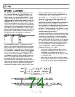
ADV7180
PIXEL PORT CONFIGURATION
The ADV7180 has a very flexible pixel port that can be
configured in a variety of formats to accommodate downstream
ICs. Table 96, Table 97, and Table 98 summarize the various
functions that the ADV7180 pins can have in different modes of
operation.
SWPC, Swap Pixel Cr/Cb, Address 0x27 [7]
This bit allows Cr and Cb samples to be swapped.
When SWPC is 0 (default), no swapping is allowed.
When SWPC is 1, the Cr and Cb values can be swapped.
The ordering of components, for example, Cr vs. Cb for
Channels A, B, and C can be changed. Refer to the SWPC, Swap
Pixel Cr/Cb, Address 0x27 [7] section. Table 96 indicates the
default positions for the Cr/Cb components.
LLC_PAD_SEL[2:0], LLC1 Output Selection,
Address 0x8F [6:4]
The following I2C write allows the user to select between LLC1
(nominally at 27 MHz) and LLC2 (nominally at 13.5 MHz).
OF_SEL[3:0], Output Format Selection, Address 0x03 [5:2]
The LLC2 signal is useful for LLC2-compatible wide bus
(16-bit) output modes. See the OF_SEL[3:0], Output Format
Selection, Address 0x03 [5:2] section for additional information.
The LLC2 signal and data on the data bus are synchronized.
By default, the rising edge of LLC1/LLC2 is aligned with the
Y data; the falling edge occurs when the data bus holds C data.
The polarity of the clock, and therefore the Y/C assignments to
the clock edges, can be altered by using the polarity LLC pin.
The modes in which the ADV7180 pixel port can be configured
are under the control of OF_SEL[3:0]. See Table 98 for details.
The default LLC frequency output on the LLC1 pin is approxi-
mately 27 MHz. For modes that operate with a nominal data rate
of 13.5 MHz (0001, 0010), the clock frequency on the LLC1 pin
stays at the higher rate of 27 MHz. For information on outputting
the nominal 13.5 MHz clock on the LLC1 pin, see the section
LLC_PAD_SEL[2:0], LLC1 Output Selection,
When LLC_PAD_SEL is 000, the output is nominally 27 MHz
LLC on the LLC1 pin (default).
Address 0x8F [6:4].
When LLC_PAD_SEL is 101, the output is nominally 13.5 MHz
LLC on the LLC2 pin.
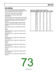
Table 96. ADV7180 LQFP-64 P15 to P0 Output/Input Pin Mapping
Data Port Pins P[15:0]
Format and Mode
15
14
13
12
11
10
9
8
7
6
5
4
3
2
1
0
Video Out, 8-Bit, 4:2:2
Video Out, 16-Bit, 4:2:2
YCrCb[7:0]OUT
Y[7:0]OUT
CrCb[7:0]OUT
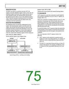
Table 97. ADV7180 LFCSP-40 P7 to P0 Output/Input Pin Mapping
Data Port Pins P[7:0]
Format and Mode
7
6
5
4
3
2
1
0
Video Out, 8-Bit, 4:2:2
YCrCb[7:0]OUT
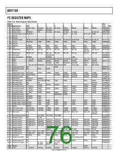
Table 98. ADV7180 Standard Definition Pixel Port Modes
ADV7180 LQFP-64 P[15: 0]
P[15:8] P[7: 0]
ADV7180 LFCSP-40
P[7: 0]
OF_SEL[3:0]
0000 to 0001
0010
0011 (Default)
0100 to 1111
Format
Reserved
Reserved, do not use
16-bit @ LLC2 4:2:2
8-bit @ LLC1 4:2:2 (default)
Reserved
Y[7:0]
CrCb[7:0]
Not valid
YCrCb[7:0]
YCrCb[7:0]
Three-state
Reserved, do not use
Rev. A | Page 72 of 112

 ADI [ ADI ]