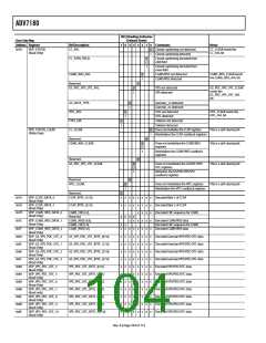
ADV7180
PCB LAYOUT RECOMMENDATIONS
Experience has repeatedly shown that the noise performance is
the same or better with a single ground plane. Using multiple
ground planes can be detrimental because each separate ground
plane is smaller, and long ground loops can result.
The ADV7180 is a high precision, high speed, mixed-signal
device. To achieve the maximum performance from the part, it
is important to have a well laid out PCB. The following is a
guide for designing a board using the ADV7180.
When using separate ground planes is unavoidable, placing a single
ground plane under the ADV7180 is recommended. The location
of the split should be under the ADV7180. In this case, it is even
more important to place components wisely because the current
loops are much longer, and current takes the path of least
resistance. An example of a current loop is a power plane to the
ADV7180 to the digital output trace to the digital data receiver to
the digital ground plane to the analog ground plane.
ANALOG INTERFACE INPUTS
Care should be taken when routing the inputs on the PCB.
Track lengths should be kept to a minimum, and 75 Ω trace
impedances should be used when possible. In addition, trace
impedances other than 75 Ω increase the chance of reflections.
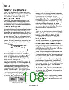
POWER SUPPLY DECOUPLING
It is recommended to decouple each power supply pin with
0.1 μF and 10 nF capacitors. The fundamental idea is to have a
decoupling capacitor within about 0.5 cm of each power pin.
Also avoid placing the capacitor on the opposite side of the PCB
from the ADV7180, because doing so interposes resistive vias in
the path. The decoupling capacitors should be located between
the power plane and the power pin. Current should flow from
the power plane to the capacitor and then to the power pin. Do
not make the power connection between the capacitor and the
power pin. Placing a via underneath the 100 nF capacitor pads,
down to the power plane, is generally the best approach (see
Figure 51).
PLL
Place the PLL loop filter components as close as possible to the
ELPF pin. It should also be placed on the same side of the PCB
as the ADV7180. Do not place any digital or other high
frequency traces near these components. Use the values
suggested in the data sheet with tolerances of 10% or less.
VREFN AND VREFP
The circuit associated with these pins should be placed as close
as possible and on the same side of the PCB as the ADV7180.
DIGITAL OUTPUTS (BOTH DATA AND CLOCKS)
VDD
VIA TO SUPPLY
Try to minimize the trace length that the digital outputs have to
drive. Longer traces have higher capacitance, requiring more
current and in turn causing more internal digital noise. Shorter
traces reduce the possibility of reflections.
10nF
100nF
GND
VIA TO GND
Adding a 30 Ω to 50 Ω series resistor can suppress reflections,
reduce EMI, and reduce the current spikes inside the ADV7180.
If series resistors are used, place them as close as possible to the
ADV7180 pins. However, try not to add vias or extra length to
the output trace to make the resistors closer.
Figure 51. Recommended Power Supply Decoupling
It is particularly important to maintain low noise and good
stability of PVDD. Careful attention must be paid to regulation,
filtering, and decoupling. It is highly desirable to provide
separate regulated supplies for each of the analog circuitry
groups (AVDD, DVDD, DVDDIO, and PVDD).
If possible, limit the capacitance that each of the digital outputs
drives to less than 15 pF. This can easily be accomplished by
keeping traces short and by connecting the outputs to only one
device. Loading the outputs with excessive capacitance increases
the current transients inside the ADV7180, creating more
digital noise on its power supplies.
Some graphic controllers use substantially different levels of
power when active (during active picture time) and when idle
(during horizontal and vertical sync periods). This can result in
a measurable change in the voltage supplied to the analog
supply regulator, which can in turn produce changes in the
regulated analog supply voltage. This can be mitigated by
regulating the analog supply, or at least PVDD, from a different,
cleaner power source, for example, from a 12 V supply.
The ADV7180 LFCSP-40 has an exposed metal paddle on the
bottom of the LFCSP package. This paddle must be soldered to
PCB ground for proper heat dissipation and also for noise and
mechanical strength benefits.
Using a single ground plane for the entire board is also
recommended. This ground plane should have a space between
the analog and digital sections of the PCB (see Figure 52).
DIGITAL INPUTS
The digital inputs on the ADV7180 are designed to work with
3.3 V signals and are not tolerant of 5 V signals. Extra
components are needed if 5 V logic signals are required to be
applied to the decoder.
ADV7180
ANALOG
SECTION
DIGITAL
SECTION
Figure 52. PCB Ground Layout
Rev. A | Page 108 of 112

 ADI [ ADI ]