ADSY8401
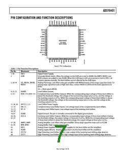
PIN CONFIGURATION AND FUNCTION DESCRIPTIONS
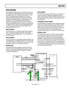
48 47 46 45 44 43 42 41 40 39 38 37
DVCC
GSW
1
2
3
4
5
6
7
8
9
36 AVCCL3
35 DO1
SEL
34 DO2
AGNDL
DO9T
33 DO3
32 DO4
ADSY8401
TOP VIEW
(Not to Scale)
DO9C
DO10T
DO10C
DO11T
31 AGNDL
30 AVCCL2
29 DO5
28 DO6
DO11C 10
AVCCL1 11
DI11 12
27 DO7
26 DO8
25 AGNDL
13 14 15 16 17 18 19 20 21 22 23 24
Figure 2. Pin Configuration
Table 3. Pin Function Descriptions
Pin No.
1, 18
2
Mnemonic
Description
DVCC
GSW
Digital Power Supply.
Grounded Mode Switch. When the voltage on the GSW pin is tied to DGND, the AMPO, MUXO, and
BFRO outputs are pulled to near AGND. When the GSW input is left unconnected or tied to DVCC, all
outputs operate normally. The level shifters are not affected by the GSW input.
3, 39–41
SEL, MUXA, MUXB,
MUXO
Analog Precharge. Low offset unity gain amplifier with MUXed inputs. Drives large capacitive loads. For
driving large capacitive loads at high slew rates, connect MUXO to BFRI and the load capacitance to
BFRO.
SEL = HIGH selects MUXA.
Level Shifter Ground.
4, 25, 31
5–10
AGNDL
DO9–11T, DO9–11C Complementary Level Shifter Outputs. While the corresponding input voltage of these level shifters is
below the threshold voltage, the voltage at the noninverting output pins is at VOL and the voltage at
the inverting outputs is at VOH. While the corresponding input voltage of these level shifters is above
the threshold voltage, the voltage at the noninverting output pins is at VOH and the voltage at the
inverting outputs is at VOL
.
11, 30, 36
12–14
15–17,
20–24
AVCCL1, 2, 3
DI9–11
DI1–8
Level Shifter Power Supply.
Complementary Level Shifter Inputs. Low voltage input of the complementary level shifters.
Inverting Level Shifter Inputs. Low voltage input of the inverting level shifters.
19, 47
26–29,
32–35
DGND
DO1-8
Digital Ground. This pin is normally connected to the digital ground plane.
Inverting Level Shifter Outputs. While the corresponding input voltage of these level shifters is below
the threshold voltage, the output voltage at these pins is at VOH. While the corresponding input voltage
of these level shifters is above the threshold voltage, the output voltage at these pins is at VOL
Analog Amplifier. Low offset unity gain amplifier. Drives large capacitive loads such as VCOM.
Analog Buffer. High current output buffer.
Analog Power Supplies. Analog power supplies for the level shifter and the amplifiers.
Analog Supply Returns. Analog supply returns for the level shifter and the amplifiers.
.
37–38
42, 44
43
AMPO, AMPI
BFRI, BFRO
AVCC
45
AGND
46
48
DTCTO
DTCTI
Edge Detecting Level Shifter Output. Logic output of the inverting level shifting edge detector.
Edge Detecting Level Shifter Input. High voltage input of the inverting level shifting edge detector.
Rev. 0 | Page 7 of 16

 ADI [ ADI ]