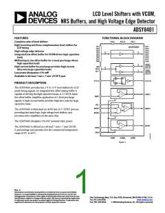
ADSY8401
Parameter
Conditions
Min
Typ
Max
Unit
BFR Section
INPUT/OUTPUT CHARACTERISTICS
Voltage Range
VH
VL
AVCC − VH
VL − AGND
GSW = LOW
1.5
1.1
90
0.3
100
6
2.5
1.5
V
V
Output Voltage Grounded Mode
Input Current
Output Current
Output Offset Voltage
Output Offset Voltage
PSRR, TA min to TA max
Gain Error, TA min to TA max
OUTPUT DYNAMIC PERFORMANCE
−3 dB Bandwidth (Small Signal)
Slew Rate
mV
µA
mA
mV
mV
mV/V
ꢀ
BFRI = 7.5 V, TA = 25°C
BFRI = 7.5 V, TA min to TA max
AVCC 10ꢀ
BFRI = 1.5 V to 12 V
VO = 6 V step, CL = 10 nF
VO = 0.25 V p-p
20
30
1
0.5
0.65
1.3
12
0.7
0.3
MHz
V/µs
µs
Settling Time to 0.5ꢀ
Overshoot
TA min to TA max
1
ꢀ
See Figure 4
CL = 10 nF
MUX and BFR Sections as NRS Buffer
Settling Time to 0.5ꢀ
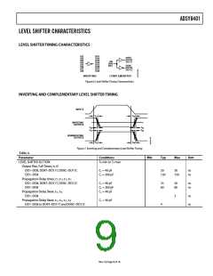
Level Shifter Section
LEVEL SHIFTER LOGIC INPUTS
CIN
IIH
IIL
VIH
0.9
1.5
3
µs
pF
µA
µA
V
0.05
−0.6
2
VIL
VTH
0.8
0.5
V
V
1.65
LEVEL SHIFTER OUTPUTS
VOH
VOL
AVCCL − 0.5
AVCCL − 0.25
0.25
V
V
LEVEL SHIFTER DYNAMIC PERFORMANCE
Output Rise, Fall Times, tr, tf
DO1–DO8, DO9T–DO11T, DO9C–DO11C
DO1–DO8
TA min to TA max
10ꢀ to 90ꢀ
CL = 40 pF
20
130
30
150
ns
ns
CL = 300 pF
Propagation Delay times, t11, t12, t13, t14
DO1–DO8, DO9T–DO11T, DO9C–DO11C
DO1–DO8
Propagation Delay Skew, t15, t16
DO1–DO8
CL = 40 pF
CL = 300 pF
CL = 40 pF
23
60
50
80
ns
ns
2
ns
ns
Propagation Delay Skew, t15, t16, t17, t18
DO1–DO8, DO9T–DO11T, DO9C–DO11C
CL = 40 pF
4
Rev. 0 | Page 4 of 16

 ADI [ ADI ]