ADSY8401
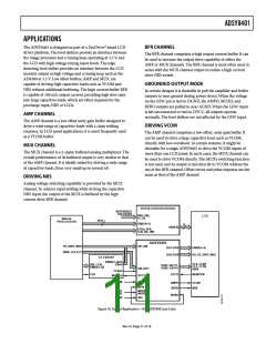
APPLICATIONS
The ADSY8401 is designed as part of a DecDriver® based LCD
driver platform. The level shifters provide an interface between
the image processor and a timing loop, operating at 3.3 V, and
the LCD with high voltage timing input levels. The edge
detecting level shifter provides an interface between the LCD
monitor output at high voltage and a timing loop such as the
AD8389 at 3.3 V. Low offset buffers, AMP and MUX, are
capable of driving high capacitive loads such as VCOM and
NRS without additional buffering. The high current buffer BFR
is capable of 100 mA output current, providing high slew rates
into large capacitive loads, which are often required for the
precharge input, NRS of LCDs.
BFR CHANNEL
The BFR channel comprises a high output current buffer. It can
be used to increase the output drive capability of either the
AMP or MUX channels. The BFR channel is most often used in
series with the MUX channel output to realize a high current
drive NRS switch.
GROUNDED OUTPUT MODE
In certain designs it is desirable to pull the amplifier and buffer
outputs to near ground during power-down. When the voltage
on the GSW pin is tied to DGND, the AMPO, MUXO, and
BFRO outputs are pulled to near AGND. When the GSW input
is left unconnected or tied to DVCC, all outputs operate
normally. The level shifters are not affected by the GSW input.
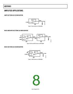
AMP CHANNEL
The AMP channel is a low offset unity gain buffer designed to
drive a wide range of capacitive loads with a clean settling
response. In LCD panel applications, it is most frequently used
as a VCOM buffer.
DRIVING VCOM
The AMP channel comprises a low offset, unity gain buffer. It
can be used to drive a large capacitive load, such as VCOM,
directly with low overshoot. In certain systems, it might be
desirable for a single ADSY8401 to drive the VCOM inputs of
more than one LCD panel. In such cases, the MUX channel can
be used to drive VCOM directly. The MUX’s switching function
is not used, and its output is tied directly to VCOM without the
use of the BFR channel. Offset errors and pulse response are the
same as that of the AMP channel.
MUX CHANNEL
The MUX channel is a 2-input, buffered analog multiplexer. The
overall performance of its buffered output is very similar to that
of the AMP channel. It is ideally suited for driving a wide range
of capacitive loads, from very small up to several nF.
DRIVING NRS
Analog voltage switching capability is provided by the MUX
channel. To achieve rapid settling while driving the capacitive
NRS input, the output of the MUX is buffered by the high
current drive BFR channel.
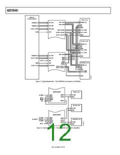
AD8381/AD8382/AD8383
REFERENCE
VOLTAGES
VRH, VRL,
V1, V2
LCD
IMAGE
10/12
PROCESSOR
DB(0:9/11)
6
VID(0:6)
STSQ, XFR,
CLK, R/L, INV
ADSY8401
DY, DIRY, NRG
DI1–DI8
DO1–DO4
ENBX(1–4)
DIRX, CLX,CLY
1/3 AD8389
ENBX(1–4)xO
DO5–DO8
DX, DY, DIRY, NRG
CLX, CLXN
CLY, CLYN
DIRX
DXI, CLXI,
DXxO
DO9T–DO11T,
DO9C–DO11C
ENBX(1–4)I
DI9–DI11
DTCTO
CLXxO
CLK
DTCTI
MONITOR
MONITxI
VCOM
AMPI
BFRI
AMPO
BFRO
VCOM
NRS
NRS1
NRS2
MUXA
MUXB
MUXO
INV
SEL
Figure 10. Typical Application—One ADSY8401 per Color
Rev. 0 | Page 11 of 16

 ADI [ ADI ]