ADSY8401
PCB DESIGN FOR OPTIMIZED THERMAL PERFORMANCE
Solder Masking
The total maximum power dissipation of the ADSY8401 is
partly load-dependent. In a typical 60 Hz XGA system, the total
maximum power dissipation is ≈ 1 W. The ADSY8401 package
is designed to provide superior thermal characteristics, partly
through the exposed die paddle on the bottom surface of the
package. To take full advantage of this feature, the exposed
paddle must be in direct thermal contact with the PCB, which
then serves as a heat sink.
To minimize the formation of solder voids due to solder flowing
into the via holes (solder wicking), the via diameter should be
small. Solder masking of the via holes on the top layer of the
PCB plugs the via holes, inhibiting solder flow into the holes. To
optimize the thermal pad coverage, the solder mask diameter
should be no more than 0.1 mm larger than the via diameter.
Table 7. Recommended Solder Mask Dimensions
Solder Mask
Top layer
Pads
Dimensions
A thermally effective PCB must incorporate a thermal pad and
a thermal via structure. The thermal pad provides a solderable
contact surface on the top surface of the PCB. The thermal via
structure provides a thermal path to the inner and bottom
layers of the PCB to remove heat.
Set by customer’s PCB design rules
0.25 mm diameter circular mask centered
on the vias
Thermal vias
Bottom layer
Set by customer’s PCB design rules
Thermal Pad Design
To minimize thermal performance degradation of production
PCBs, the contact area between the thermal pad and the PCB
should be maximized. Therefore, the size of the thermal pad on
the top PCB layer should match the exposed paddle. The second
thermal pad of the same size should be placed on the bottom
side of the PCB. At least one thermal pad should be in direct
thermal contact with an external plane such as AVCC or GND.
7mm
Thermal Via Structure Design
Effective heat transfer from the top to the inner and bottom
layers of the PCB requires thermal vias incorporated into the
thermal pad design. Thermal performance increases logarith-
mically with the number of vias. Near optimum thermal
performance of production PCBs is attained only when tightly
spaced thermal vias are placed on the full extent of the thermal
pad.
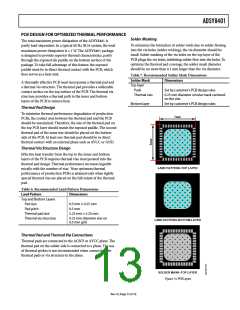
LAND PATTERN–TOP LAYER
Table 6. Recommended Land Pattern Dimensions
Land Pattern
Dimensions
Top and Bottom Layers
Pad size
Pad pitch
0.5 mm × 0.25 mm
0.5 mm
Thermal pad size
Thermal via structure
5.25 mm × 5.25 mm
0.25 mm diameter vias on
0.5 mm grid
LAND PATTERN–BOTTOM LAYER
Thermal Pad and Thermal Via Connections
Thermal pads are connected to the AGND or AVCC plane. The
thermal pad on the solder side is connected to a plane. The use
of thermal spokes is not recommended when connecting the
thermal pads or via structure to the plane.
SOLDER MASK–TOP LAYER
Figure 13. PCB Layers
Rev. 0 | Page 13 of 16

 ADI [ ADI ]