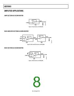
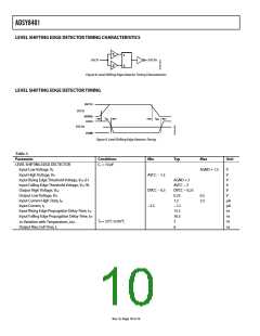
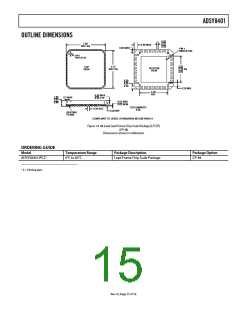
ADSY8401
Layout and Grounding
POWER SUPPLY SEQUENCING
The analog outputs and the digital inputs of the ADSY8401 are
on opposite sides of the package. Keep these sections separated
to minimize crosstalk and coupling of digital inputs into the
analog outputs.
As indicated in the Absolute Maximum Ratings section, the
voltage at any input pin cannot exceed its supply voltage by
more than 0.5 V. To ensure compliance with the absolute
maximum ratings, power-up and power-down sequencing
might be required.
All signal trace lengths should be made as short and direct as
possible to prevent signal degradation due to parasitic effects.
Note that a digital signal should not cross or be routed near
analog signals.
During power-up, initial application of nonzero voltages to any
of the input pins must be delayed until the supply voltage ramps
up to at least the highest maximum operational input voltage.
It is imperative to provide a solid analog ground plane under
and around the ADSY8401. All ground pins of the part should
be connected directly to this ground plane with no extra signal
path length. This includes AGND, AGNDL, and DGND. The
return traces for any of the signals should be routed close to the
ground pin for that section to prevent stray signals from
coupling into other ground pins.
During power-down, the voltage at any input pin must reach
zero during a period not exceeding the hold-up time of the
power supply.
Failure to comply with the absolute maximum ratings may
result in functional failure or damage to the internal ESD
diodes. Damaged ESD diodes can cause temporary parametric
failures, which can result in image artifacts. Damaged ESD
diodes cannot provide full ESD protection, reducing reliability.
Power Supply Bypassing
All power supply pins of the ADSY8401 must be properly
bypassed to the analog ground plane for optimum performance.
Power-on sequence:
TOTAL POWER DISSIPATION
1. Apply power to supplies.
2. Apply inputs.
The total power dissipation of the ADSY8401 has three
components:
Power-off sequence:
•
•
Quiescent power dissipation when all digital inputs are low.
1. Remove signal from inputs.
Dynamic power dissipation due to the capacitance of
the LCD (typical CL = 200 pF for all the NRG control inputs,
CL = 40 pF for all other control inputs).
2. Remove power from supplies.
Power-Off Sequencing Using the GSW Pin
In certain designs it is desirable to pull the amplifier, buffer, and
level shifter outputs to near ground during power-down.
•
Average power dissipation due to the toggling inputs.
When DI1–DI11 are at digital low, the quiescent power dissipa-
tion of the ADSY8401 is 576 mW. When DI1–DI11 are at digital
high, the quiescent power dissipation is 771 mW.
Power-off sequence with GSW:
1. Apply low to the GSW pin.
The typical dynamic power dissipation of each of the three
ADSY8401, due to the capacitance of the LCD, is 155 mW in a
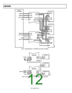
typical 60 Hz XGA system, shown in Figure 10. It is 304 mW
and 153 mW, respectively, for the two ADSY8401s in the 60 Hz
XGA system shown in Figure 11.
2. Apply high to all level shifter input pins.
3. Pull the MUXA, MUXB, AMPI, and BFRI inputs to AGND.
4. Remove AVCC.
5. Remove DVCC.
The average power dissipation of each of the three ADSY8401
due to DI1–DI11 toggling is 23 mW in the system shown in
Figure 10. It is 32 mW and 22 mW, respectively, for the two
ADSY8401 in the system shown in Figure 11.
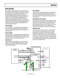
LAYOUT CONSIDERATIONS
The ADSY8401 is a mixed-signal, high speed, high accuracy
device. To fully realize its specifications, it is essential to use a
properly designed printed circuit board.
The total power dissipation of each of the three ADSY8401 in
the XGA system, shown in Figure 10, is 754 mW.
The total power dissipation of the two ADSY8401s in the XGA
system, shown in Figure 12, is 912 mW and 751 mW,
respectively.
Rev. 0 | Page 14 of 16

 ADI [ ADI ]