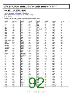
ADSP-BF542/ADSP-BF544/ADSP-BF547/ADSP-BF548/ADSP-BF549
TEST CONDITIONS
REFERENCE
SIGNAL
All timing parameters appearing in this data sheet were mea-
sured under the conditions described in this section. Figure 71
shows the measurement point for AC measurements (except
tDIS_MEASURED
tENA_MEASURED
output enable/disable). The measurement point VMEAS is
tDIS
tENA
VDDEXT/2 or VDDDDR/2, depending on the pin under test.
V
OH
V
(MEASURED)
OH
(MEASURED)
V
(MEASURED) ꢂ ꢃV
(MEASURED) + ꢃV
OH
V
(HIGH)
TRIP
V
(LOW)
V
V
TRIP
OL
INPUT
V
OL
(MEASURED)
OL
OR
OUTPUT
V
V
MEAS
(MEASURED)
MEAS
tDECAY
tTRIP
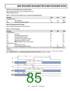
Figure 71. Voltage Reference Levels for AC Measurements
(Except Output Enable/Disable)
OUTPUT STOPS DRIVING
OUTPUT STARTS DRIVING
HIGH IMPEDANCE STATE
Output Enable Time
Figure 72. Output Enable/Disable
Output pins are considered to be enabled when they have made
a transition from a high-impedance state to the point when they
start driving. The output enable time tENA is the interval from
the point when a reference signal reaches a high or low voltage
level to the point when the output starts driving as shown in the
output enable/disable diagram (Figure 72). The time,
tENA_MEASURED, is the interval from the point when the reference
signal switches to the point when the output voltage reaches
either 1.75 V (output high) or 1.25 V (output low). Time tTRIP is
the interval from when the output starts driving to when the
output reaches the 1.25 V or 1.75 V trip voltage. Time tENA is
calculated as shown in the equation:
Example System Hold Time Calculation
To determine the data output hold time in a particular system,
first calculate tDECAY using the equation given above. Choose ∆V
to be the difference between the ADSP-BF54x Blackfin proces-
sors’ output voltage and the input threshold for the device
requiring the hold time. A typical ∆V will be 0.4 V. CL is the total
bus capacitance (per data line), and IL is the total leakage or
three-state current (per data line). The hold time will be tDECAY
plus the minimum disable time (for example, tDDAT for an asyn-
chronous memory write cycle).
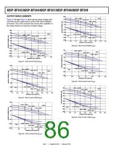
CAPACITIVE LOADING
Output delays and holds are based on standard capacitive loads
of an average of 6 pF on all balls (see Figure 73).
t
= t
– t
ENA_MEASURED TRIP
ENA
If multiple pins (such as the data bus) are enabled, the measure-
ment value is that of the first pin to start driving.
TESTER PIN ELECTRONICS
50:
Output Disable Time
V
LOAD
T1
DUT
Output pins are considered to be disabled when they stop driv-
ing, go into a high-impedance state, and start to decay from
their output high or low voltage. The time for the voltage on the
bus to decay by ∆V is dependent on the capacitive load, CL and
the load current, IL. This decay time can be approximated by the
equation:
OUTPUT
45:
70:
ZO = 50:ꢀ(impedance)
TD = 4.04 r 1.18 ns
50:
0.5pF
4pF
2pF
400:
t
= (C ∆V) ⁄ I
DECAY
L
L
The output disable time tDIS is the difference between
NOTES:
THE WORST-CASE TRANSMISSION LINE DELAY IS SHOWN AND CAN BE USED
FOR THE OUTPUT TIMING ANALYSIS TO REFELECT THE TRANSMISSION LINE
EFFECT AND MUST BE CONSIDERED.THE TRANSMISSION LINE (TD), IS FOR
LOAD ONLY AND DOES NOT AFFECT THE DATA SHEET TIMING SPECIFICATIONS.
t
DIS_MEASURED and tDECAY as shown in Figure 72. The time
DIS_MEASURED is the interval from when the reference signal
t
switches to when the output voltage decays ∆V from the mea-
sured output high or output low voltage. The time tDECAY is
calculated with test loads CL and IL, and with ∆V equal to 0.25 V.
ANALOG DEVICES RECOMMENDS USING THE IBIS MODEL TIMING FOR A GIVEN
SYSTEM REQUIREMENT. IF NECESSARY, A SYSTEM MAY INCORPORATE
EXTERNAL DRIVERS TO COMPENSATE FOR ANY TIMING DIFFERENCES.
Figure 73. Equivalent Device Loading for AC Measurements
(Includes All Fixtures)
Rev. C
|
Page 88 of 100
|
February 2010

 ADI [ ADI ]