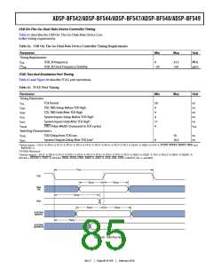
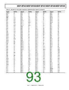
ADSP-BF542/ADSP-BF544/ADSP-BF547/ADSP-BF548/ADSP-BF549
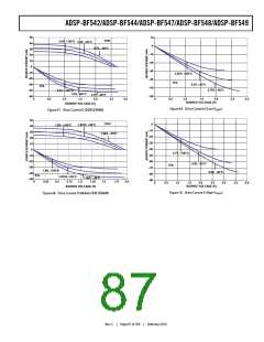
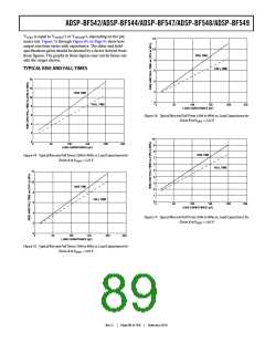
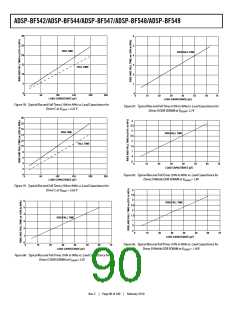
VLOAD is equal to VDDEXT/2 or VDDDDR/2, depending on the pin
12
under test. Figure 74 through Figure 85 on Page 91 show how
output rise time varies with capacitance. The delay and hold
specifications given should be derated by a factor derived from
these figures. The graphs in these figures may not be linear out-
side the ranges shown.
10
RISE TIME
8
6
4
2
0
FALL TIME
TYPICAL RISE AND FALL TIMES
14
12
RISE TIME
10
FALL TIME
0
50
100
150
200
250
8
LOAD CAPACITANCE (pF)
6
4
Figure 76. Typical Rise and Fall Times (10% to 90%) vs. Load Capacitance for
Driver B at VDDEXT = 2.25 V
2
0
10
0
50
100
150
200
250
9
8
LOAD CAPACITANCE (pF)
RISE TIME
Figure 74. Typical Rise and Fall Times (10% to 90%) vs. Load Capacitance for
Driver A at VDDEXT = 2.25 V
7
6
FALL TIME
5
12
4
3
2
1
0
10
RISE TIME
8
FALL TIME
6
0
50
100
150
200
250
LOAD CAPACITANCE (pF)
4
2
0
Figure 77. Typical Rise and Fall Times (10% to 90%) vs. Load Capacitance for
Driver B at VDDEXT = 3.65 V
0
50
100
150
200
250
LOAD CAPACITANCE (pF)
Figure 75. Typical Rise and Fall Times (10% to 90%) vs. Load Capacitance for
Driver A at VDDEXT = 3.65 V
Rev. C
|
Page 89 of 100
|
February 2010

 ADI [ ADI ]