ADM8690–ADM8695
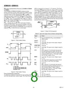
(PFI) is compared to an internal +1.3 V reference. T he Power
Fail Output (PFO) goes low when the voltage at PFI is less than
1.3 V. T ypically PFI is driven by an external voltage divider that
senses either the unregulated dc input to the system’s 5 V regu-
lator or the regulated 5 V output. T he voltage divider ratio can
be chosen such that the voltage at PFI falls below 1.3 V several
milliseconds before the +5 V power supply falls below the reset
threshold. PFO is normally used to interrupt the microprocessor
so that data can be stored in RAM and the shut down procedure
executed before power is lost
CE Gating and RAM Wr ite P r otection (AD M8691/AD M8693/
AD M8695)
T he ADM8691/ADM8693/ADM8695 products include
memory protection circuitry which ensures the integrity of data
in memory by preventing write operations when VCC is at an in-
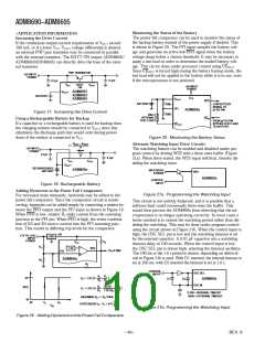
valid level. T here are two additional pins, CEIN and CEOUT
,
which may be used to control the Chip Enable or Write inputs
of CMOS RAM. When VCC is present, CEOUT is a buffered rep-
lica of CEIN, with a 3 ns propagation delay. When VCC falls be-
low the reset voltage threshold or VBAT T, an internal gate forces
CEOUT high, independent of CEIN
.
INPUT
POWER
ADM869x
CEOUT typically drives the CE, CS or write input of battery
backed up CMOS RAM. T his ensures the integrity of the data
in memory by preventing write operations when VCC is at an in-
valid level. Similar protection of EEPROMs can be achieved by
using the CEOUT to drive the store or write inputs.
R1
R2
1.3V
POWER
FAIL
PFO
OUTPUT
POWER
FAIL
INPUT
Figure 7. Power Fail Com parator
Table II. Input and O utput Status In Battery Backup Mode
ADM869x
CE
IN
CE
OUT
Signal
Status
V
V
LOW = 0
OK = 1
CC
CC
VOUT
VOUT is connected to VBAT T via an internal
PMOS switch.
Figure 5. Chip Enable Gating
RESET
Logic low.
RESET
Logic high. T he open circuit output voltage is
V2
V2
equal to VOUT
.
V
V1
V1
CC
LOW LINE
Logic low.
BAT T ON
Logic high. T he open circuit voltage is equal to
VOUT.
t1
t1
RESET
WDI
WDI is ignored. It is internally disconnected
from the internal pull-up resistor and does not
source or sink current as long as its input voltage
is between GND and VOUT . T he input voltage
does not affect supply current.
LOW LINE
WDO
Logic high. T he open circuit voltage is equal
to VOUT
.
CE
IN
PFI
T he Power Fail Comparator is turned off and
has no effect on the Power Fail Output.
PFO
CEIN
Logic low.
CE
OUT
CEIN is ignored. It is internally disconnected
from its internal pull-up and does not source or
sink current as long as its input voltage is
between GND and VOUT . T he input voltage
does not affect supply current.
t1 = RESET TIME
V1 = RESET VOLTAGE THRESHOLD LOW
V2 = RESET VOLTAGE THRESHOLD HIGH
HYSTERESIS = V2–V1
CEOUT
Logic high. T he open circuit voltage is equal to
Figure 6. Chip Enable Tim ing
P ower Fail War ning Com par ator
An additional comparator is provided for early warning of fail-
ure in the microprocessor’s power supply. T he Power Fail Input
VOUT
.
OSC IN
OSC IN is ignored.
OSC SEL is ignored.
OSC SEL
–8–
REV. 0

 ADI [ ADI ]