ADM8690–ADM8695
Monitor ing the Status of the Batter y
+AP P LICATIO N INFO RMATIO N
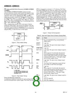
T he power fail comparator can be used to monitor the status of
the backup battery instead of the power supply if desired. T his
is shown in Figure 20. T he PFI input samples the battery volt-
age and generates an active low PFO signal when the battery
voltage drops below a chosen threshold. It may be necessary to
apply a test load in order to determine the loaded battery volt-
age. T his can be done under processor control using CEOUT .
Since CEOUT is forced high during the battery backup mode, the
test load will not be applied to the battery while it is in use, even
if the microprocessor is not powered.
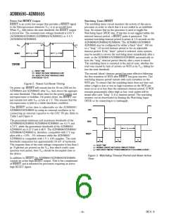
Incr easing the D r ive Cur r ent
If the continuous output current requirements at VOUT exceed
100 mA, or if a lower VCC–VOUT voltage differential is desired,
an external PNP pass transistor may be connected in parallel
with the internal transistor. T he BAT T ON output (ADM8691/
ADM8693/ADM8695) can directly drive the base of the exter-
nal transistor.
PNP TRANSISTOR
+5V INPUT
POWER
0.1µF
0.1µF
V
BATT
ON
V
OUT
CC
+5V INPUT
POWER
V
ADM8691
ADM8693
ADM8695
BATT
BATTERY
V
CC
V
BATT
PFO
BATTERY
10MΩ
10MΩ
LOW BATTERY
SIGNAL TO
µP I/O PIN
PFI
ADM869x
Figure 17. Increasing the Drive Current
20kΩ
OPTIONAL
TEST LOAD
CE
IN
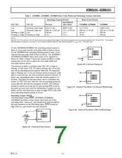
Using a Rechar geable Batter y for Backup
FROM µP I/O PIN
APPLIES TEST LOAD
TO BATTERY
If a capacitor or a rechargeable battery is used for backup then
the charging resistor should be connected to VOUT since this
eliminates the discharge path that would exist during power-
CE
OUT
down if the resistor is connected to VCC
.
Figure 20. Monitoring the Battery Status
V
– V
BATT
OUT
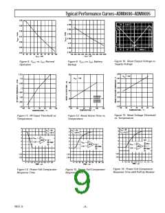
Alter nate Watchdog Input D r ive Cir cuits
I =
R
+5V INPUT
POWER
T he watchdog feature can be enabled and disabled under pro-
gram control by driving WDI with a three-state buffer (Figure
21a). When three-stated, the WDI input will float, thereby dis-
abling the watchdog timer.
0.1µF
R
0.1µF
V
V
OUT
CC
V
BATT
RECHARGEABLE
BATTERY
ADM869x
WATCHDOG
WDI
STROBE
ADM869x
CONTROL
INPUT
Figure 18. Rechargeable Battery
Adding H yster esis to the P ower Fail Com par ator
Figure 21a. Program m ing the Watchdog Input
For increased noise immunity, hysteresis may be added to the
power fail comparator. Since the comparator circuit is nonin-
verting, hysteresis can be added simply by connecting a resistor be-
tween the PFO output and the PFI input as shown in Figure 19.
When PFO is low, resistor R3 sinks current from the summing
junction at the PFI pin. When PFO is high, the series combina-
tion of R3 and R4 source current into the PFI summing junc-
tion. T his results in differing trip levels for the comparator.
T his circuit is not entirely foolproof, and it is possible that a
software fault could erroneously three-state the buffer. T his
would then prevent the ADM869x from detecting that the mi-
croprocessor is no longer operating correctly. In most cases a
better method is to extend the watchdog period rather than dis-
abling the watchdog. T his may be done under program control
using the circuit shown in Figure 21b. When the control input is
high, the OSC SEL pin is low and the watchdog timeout is set
by the external capacitor. A 0.01 µF capacitor sets a watchdog
timeout delay of 100 seconds. When the control input is low,
the OSC SEL pin is driven high, selecting the internal oscillator.
The 100 ms or the 1.6 s period is chosen, depending on which di-
ode in Figure 21b is used. With D1 inserted, the internal timeout is
set at 100 ms; with D2 inserted the timeout is set at 1.6 s.
+5V
+7V TO +15V
7805
INPUT
POWER
R
V
4
CC
R
1
2
1.3V
PFO
TO µP NMI
PFI
ADM869x
R
R
3
CONTROL
OSC SEL
INPUT*
R
R
R
1
1
5V
V
V
= 1.3V
= 1.3V
(
1+
+
–
)
ADM869x
H
D 1
D 2
R
2
3
OSC IN
R
R
R
(5V – 1.3V)
1
1
PFO
(1+
)
4
L
1.3V (R + R )
2
3
*LOW = INTERNAL TIMEOUT
HIGH = EXTERNAL TIMEOUT
ASSUMING R < < R THEN
4
3
0V
R
R
0V
V
V
H
1
L
HYSTERESIS V – V = 5V
(
)
H
L
V
IN
2
Figure 21b. Program m ing the Watchdog Input
Figure 19. Adding Hysteresis to the Power Fail Com parator
–10–
REV. 0

 ADI [ ADI ]