ADM8690–ADM8695
TYP ICAL AP P LICATIO NS
AD M8690, AD M8692 and AD M8694
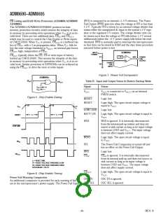
Figure 22b shows a similar application but in this case the PFI
input monitors the unregulated input to the 7805 voltage regu-
lator. T his gives an earlier warning of an impending power fail-
ure. It is useful with processors operating at low speeds or where
there are a significant number of housekeeping tasks to be com-
pleted before the power is lost.
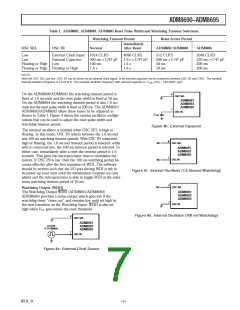
Figure 22a shows the ADM8690/ADM8692/ADM8694 in a
typical power monitoring, battery backup application. VOUT
powers the CMOS RAM. Under normal operating conditions
with VCC present, VOUT is internally connected to VCC. If a
power failure occurs, VCC will decay and VOUT will be switched
to VBAT T thereby maintaining power for the CMOS RAM. A
RESET pulse is also generated when VCC falls below 4.65 V for
the ADM8690/ADM8694 or 4.4 V for the ADM8692. RESET
will remain low for 50 ms (200 ms for ADM8694) after VCC re-
turns to 5 V.
INPUT
POWER
V > 8V
+5V
7805
0.1µF
0.1µF
R
1
2
µP POWER
CMOS RAM
V
CC
V
PFI
OUT
POWER
R
ADM8690
ADM8692
ADM8694
µP SYSTEM
T he watchdog timer input (WDI) monitors an I/O line from the
µP system. T his line must be toggled once every 1.6 seconds to
verify correct software execution. Failure to toggle the line indi-
cates that the µP system is not correctly executing its program
and may be tied up in an endless loop. If this happens, a reset
pulse is generated to initialize the processor.
µP RESET
RESET
PFO
V
BATT
µP NMI
+
BATTERY
I/O LINE
WDI
GND
Figure 22b. ADM8690/ADM8692/ADM8694 Typical Applica-
tion Circuit B
If the watchdog timer is not needed, the WDI input should be
left floating.
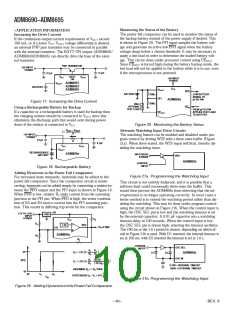
AD M8691, AD M8693 and AD M8695
A typical connection for the ADM8691/ADM8693/ADM8695
is shown in Figure 23. CMOS RAM is powered from VOUT
T he Power Fail Input, PFI, monitors the input power supply via
a resistive divider network. T he voltage on the PFI input is com-
pared with a precision 1.3 V internal reference. If the input volt-
age drops below 1.3 V, a power fail output (PFO) signal is
generated. T his warns of an impending power failure and may
be used to interrupt the processor so that the system may be
shut down in an orderly fashion. T he resistors in the sensing
network are ratioed to give the desired power fail threshold
voltage VT .
.
When 5 V power is present this is routed to VOUT . If VCC fails
then VBAT T is routed to VOUT . VOUT can supply up to 100 mA
from VCC, but if more current is required, an external PNP tran-
sistor can be added. When VCC is higher than VBAT T, the BAT T
ON output goes low, providing up to 25 mA of base drive for
the external transistor. A 0.1 µF capacitor is connected to VOUT
to supply the transient currents for CMOS RAM. When VCC is
lower than VBAT T, an internal 20 Ω MOSFET connects the
VT = (1.3 R1/R2) + 1.3 V
R1/R2 = (VT/1.3) – 1
backup battery to VOUT
.
INPUT POWER
+5V
+5V
R
R
1
V
CC
µP POWER
CMOS RAM
0.1µF
0.1µF
V
PFI
OUT
V
V
BATT
ON
CC
OUT
POWER
CMOS
RAM
ADM8690
ADM8692
ADM8694
0.1µF
CE
3V
2
OUT
V
BATT
BATTERY
µP SYSTEM
ADM8691
ADM8693
ADM8695
ADDRESS
DECODE
R
R
CE
1
IN
µP RESET
RESET
V
BATT
PFI
µP NMI
PFO
A0–A15
I/O LINE
+
GND
BATTERY
WDI
I/O LINE
2
WDI
GND
µP
NC
OSC IN
PFO
NMI
OSC SEL
RESET
RESET
LOW LINE WDO
RESET
Figure 22a. ADM8690/ADM8692/ADM8694 Typical Applica-
tion Circuit A
0.1µF
SYSTEM STATUS
INDICATORS
Figure 23. ADM8691/ADM8693/ADM8695 Typical
Application
REV. 0
–11–

 ADI [ ADI ]