ADG1419
TERMINOLOGY
IDD
t
ON (EN)
The positive supply current.
Delay time between the 50% and 90% points of the digital input
and switch on condition. See Figure 27.
ISS
The negative supply current.
tOFF (EN)
Delay time between the 50% and 90% points of the digital input
and switch off condition. See Figure 27.
VD (VS)
The analog voltage on Terminal D and Terminal S.
tTRANSITION
RON
Delay time between the 50% and 90% points of the digital
inputs and the switch on condition when switching from one
address state to another.
The ohmic resistance between Terminal D and Terminal S.
RFLAT (ON)
Flatness is defined as the difference between the maximum and
minimum value of on resistance as measured over the specified
analog signal range.
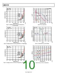
TBBM
Off time measured between the 80% point of both switches
when switching from one address state to another. See Figure 26.
IS (Off)
Charge Injection
A measure of the glitch impulse transferred from the digital
input to the analog output during switching. See Figure 28.
The source leakage current with the switch off.
ID (Off)
The drain leakage current with the switch off.
Off Isolation
ID, IS (On)
A measure of unwanted signal coupling through an off switch.
See Figure 29.
The channel leakage current with the switch on.
VINL
Crosstalk
The maximum input voltage for Logic 0.
A measure of unwanted signal that is coupled through from one
channel to another as a result of parasitic capacitance. See
Figure 30.
VINH
The minimum input voltage for Logic 1.
I
INL (IINH
)
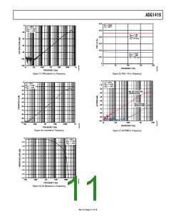
Bandwidth
The input current of the digital input.
The frequency at which the output is attenuated by 3 dB. See
Figure 31.
CS (Off)
The off switch source capacitance, measured with reference to
On Response
ground.
The frequency response of the on switch.
CD (Off)
Insertion Loss
The off switch drain capacitance, measured with reference to
The loss due to the on resistance of the switch. See Figure 31.
ground.
THD + N
CD, CS (On)
The ratio of the harmonic amplitude plus noise of the signal to
the fundamental. See Figure 32.
The on switch capacitance, measured with reference to ground.
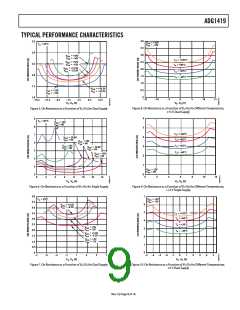
AC Power Supply Rejection Ratio (ACPSRR)
CIN
ACPSRR measures the ability of a part to avoid coupling noise and
spurious signals that appear on the supply voltage pin to the
output of the switch. The dc voltage on the device is modulated
by a sine wave of 0.62 V p-p. The ratio of the amplitude of
signal on the output to the amplitude of the modulation is the
ACPSRR. See Figure 21.
The digital input capacitance.
Rev. 0 | Page 14 of 16

 ADI [ ADI ]