Data Sheet
ADF4360-3
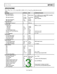
PIN CONFIGURATION AND FUNCTION DESCRIPTIONS
PIN 1
IDENTIFIER
CPGND
AV
1
2
3
4
5
6
18 DATA
17 CLK
DD
ADF4360-3
AGND
16 REF
IN
TOP VIEW
RF
A
B
15 DGND
(Not to Scale)
OUT
OUT
RF
14
13
C
R
N
V
VCO
SET
NOTES
1. THE EXPOSED PAD MUST BE CONNECTED TO AGND.
Figure 3. Pin Configuration
Table 4. Pin Function Descriptions
Pin No.
Mnemonic Function
1
2
CPGND
AVDD
Charge Pump Ground. This is the ground return path for the charge pump.
Analog Power Supply. This ranges from 3.0 V to 3.6 V. Decoupling capacitors to the analog ground plane
should be placed as close as possible to this pin. AVDD must have the same value as DVDD
.
3, 8 to 11, 22
4
AGND
Analog Ground. This is the ground return path of the prescaler and VCO.
VCO Output. The output level is programmable from –3 dBm to −12 dBm. See the Output Matching section
for a description of the various output stages.
VCO Complementary Output. The output level is programmable from −3 dBm to −12 dBm. See Output
Matching section for a description of the various output stages.
Power Supply for the VCO. This ranges from 3.0 V to 3.6 V. Decoupling capacitors to the analog ground plane
should be placed as close as possible to this pin. VVCO must have the same value as AVDD
Control Input to the VCO. This voltage determines the output frequency and is derived from filtering the CP
output voltage.
RFOUT
RFOUT
VVCO
A
5
6
7
B
.
VTUNE
12
13
CC
RSET
Internal Compensation Node. This pin must be decoupled to ground with a 10 nF capacitor.
Connecting a resistor between this pin and CPGND sets the maximum charge pump output current for the
synthesizer. The nominal voltage potential at the RSET pin is 0.6 V. The relationship between ICP and RSET is
11.75
RSET
ICPmax
=
with RSET = 4.7 kΩ, ICPmax = 2.5 mA.
14
15
16
CN
DGND
REFIN
Internal Compensation Node. This pin must be decoupled to VVCO with a 10 μF capacitor.
Digital Ground.
Reference Input. This is a CMOS input with a nominal threshold of VDD/2 and a dc equivalent input resistance of
100 kΩ. See Figure 10. This input can be driven from a TTL or CMOS crystal oscillator or it can be ac-coupled.
17
18
19
20
21
23
24
CLK
Serial Clock Input. This serial clock is used to clock in the serial data to the registers. The data is latched into
the 24-bit shift register on the CLK rising edge. This input is a high impedance CMOS input.
Serial Data Input. The serial data is loaded MSB first with the two LSBs being the control bits. This input is a
high impedance CMOS input.
Load Enable, CMOS Input. When LE goes high, the data stored in the shift registers is loaded into one of the
four latches, and the relevant latch is selected using the control bits.
This multiplexer output allows either the lock detect, the scaled RF, or the scaled reference frequency to be
accessed externally.
DATA
LE
MUXOUT
DVDD
CE
Digital Power Supply. This ranges from 3.0 V to 3.6 V. Decoupling capacitors to the digital ground plane
should be placed as close as possible to this pin. DVDD must have the same value as AVDD
.
Chip Enable. A logic low on this pin powers down the device and puts the charge pump into three-state
mode. Taking the pin high powers up the device depending on the status of the power-down bits.
Charge Pump Output. When enabled, this provides ICP to the external loop filter, which in turn drives the
internal VCO.
CP
EP
Exposed Pad. The exposed pad must be connected to AGND.
Rev. C | Page 7 of 24

 ADI [ ADI ]