ADF4360-3
Data Sheet
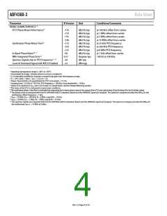
Parameter
B Version
Unit
Conditions/Comments
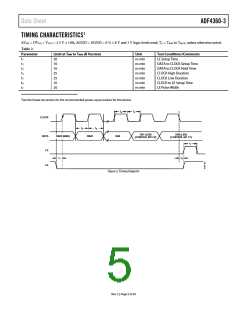
NOISE CHARACTERISTICS1, 5
VCO Phase-Noise Performance8
−110
−133
−141
−146
−172
−163
−147
−85
dBc/Hz typ
dBc/Hz typ
dBc/Hz typ
dBc/Hz typ
dBc/Hz typ
dBc/Hz typ
dBc/Hz typ
dBc/Hz typ
Degrees typ
dBc typ
@ 100 kHz offset from carrier.
@ 1 MHz offset from carrier.
@ 3 MHz offset from carrier.
@ 10 MHz offset from carrier.
@ 25 kHz PFD frequency.
@ 200 kHz PFD frequency.
@ 8 MHz PFD frequency.
@ 1 kHz offset from carrier.
100 Hz to 100 kHz.
Synthesizer Phase-Noise Floor9
In-Band Phase Noise10, 11
RMS Integrated Phase Error12
0.57
−65
Spurious Signals due to PFD Frequency11, 13
Level of Unlocked Signal with MTLD Enabled
−41
dBm typ
1 Operating temperature range is –40°C to +85°C.
2 Guaranteed by design. Sample tested to ensure compliance.
3 ICP is internally modified to maintain constant loop gain over the frequency range.
4 TA = 25°C; AVDD = DVDD = VVCO = 3.3 V; P = 32.
5 These characteristics are guaranteed for VCO core power = 15 mA.
6 Jumping from 1.6 GHz to 1.95 GHz. PFD frequency = 200 kHz; loop bandwidth = 10 kHz.
7 Using 50 Ω resistors to VVCO, into a 50 Ω load. For tuned loads, see the Output Matching section.
8 The noise of the VCO is measured in open-loop conditions.
9 The synthesizer phase -noise floor is estimated by measuring the in-band phase noise at the output of the VCO and subtracting 20 log N (where N is the N divider value).
10 The phase noise is measured with the EV-ADF4360-xEB1Z Evaluation Board and the HP8562E Spectrum Analyzer. The spectrum analyzer provides the REFIN for the
synthesizer; offset frequency = 1 kHz.
11
f
f
= 10 MHz; fPFD = 200 kHz; N = 9,000; Loop B/W = 10 kHz.
= 10 MHz; fPFD = 1 MHz; N = 1,800; Loop B/W = 25 kHz.
REFIN
12
REFIN
13 The spurious signals are measured with the EV-ADF4360-xEB1Z Evaluation Board and the HP8562E Spectrum Analyzer. The spectrum analyzer provides the REFIN for
the synthesizer; fREFOUT = 10 MHz @ 0 dBm.
Rev. C | Page 4 of 24

 ADI [ ADI ]