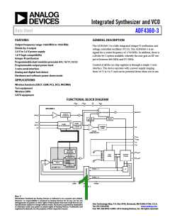
Data Sheet
ADF4360-3
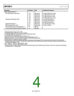
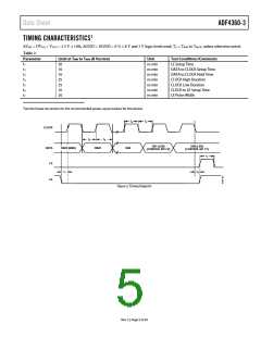
TIMING CHARACTERISTICS1
AVDD = DVDD = VVCO = 3.3 V 10%; AGND = DGND = 0 V; 1.8 V and 3 V logic levels used; TA = TMIN to TMAX, unless otherwise noted.
Table 2.
Parameter
Limit at TMIN to TMAX (B Version)
Unit
Test Conditions/Comments
LE Setup Time
t1
t2
t3
t4
t5
t6
t7
20
10
10
25
25
10
20
ns min
ns min
ns min
ns min
ns min
ns min
ns min
DATA to CLOCK Setup Time
DATA to CLOCK Hold Time
CLOCK High Duration
CLOCK Low Duration
CLOCK to LE Setup Time
LE Pulse Width
1See the Power-Up section for the recommended power-up procedure for this device.
t4
t5
CLOCK
t2
t3
DB1 (LSB)
(CONTROL BIT C2)
DB0 (LSB)
(CONTROL BIT C1)
DB23 (MSB)
DB22
DB2
DATA
LE
t7
t1
t6
LE
Figure 2. Timing Diagram
Rev. C | Page 5 of 24

 ADI [ ADI ]