AD9364
Data Sheet
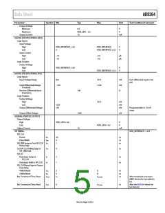
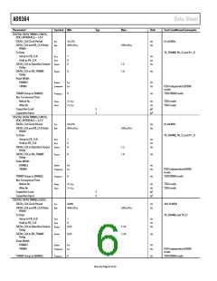
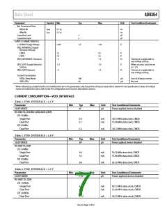
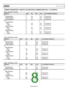
Parameter1
Symbol Min
Typ
Max
Unit
Test Conditions/Comments
TRANSMITTER, 800 MHz
Output S22
−10
8
dB
Maximum Output Power
Modulation Accuracy (EVM)
dBm
dB
1 MHz tone into 50 Ω load
19.2 MHz reference clock
−40
23
Third-Order Output Intermod-
ulation Intercept Point
OIP3
dBm
Carrier Leakage
−50
dBc
0 dB attenuation
40 dB attenuation
90 MHz offset
−32
dBc
Noise Floor
−157
dBm/Hz
TRANSMITTER, 2.4 GHz
Output S22
−10
7.5
dB
Maximum Output Power
Modulation Accuracy (EVM)
dBm
dB
1 MHz tone into 50 Ω load
40 MHz reference clock
−40
19
Third-Order Output Intermod-
ulation Intercept Point
OIP3
dBm
Carrier Leakage
−50
dBc
0 dB attenuation
40 dB attenuation
90 MHz offset
−32
dBc
Noise Floor
−156
dBm/Hz
TRANSMITTER, 5.5 GHz
Output S22
−10
6.5
dB
Maximum Output Power
Modulation Accuracy (EVM)
dBm
dB
7 MHz tone into 50 Ω load
−36
40 MHz reference clock
(doubled internally for RF
synthesizer)
Third-Order Output Intermod-
ulation Intercept Point
OIP3
17
dBm
Carrier Leakage
−50
dBc
0 dB attenuation
40 dB attenuation
90 MHz offset
−30
dBc
Noise Floor
−151.5
dBm/Hz
TX MONITOR INPUT (TX_MON)
Maximum Input Level
Dynamic Range
4
dBm
dB
66
1
Accuracy
dB
LO SYNTHESIZER
LO Frequency Step
2.4
Hz
2.4 GHz, 40 MHz reference
clock
Integrated Phase Noise
800 MHz
0.13
° rms
100 Hz to 100 MHz, 30.72 MHz
reference clock (doubled
internally for RF synthesizer)
2.4 GHz
5.5 GHz
0.37
0.59
° rms
° rms
100 Hz to 100 MHz, 40 MHz
reference clock
100 Hz to 100 MHz, 40 MHz
reference clock (doubled
internally for RF synthesizer)
REFERENCE CLOCK (REF_CLK)
REF_CLK is either the input to
the XTALP/XTALN pins or a
line directly to the XTALN pin
Input
Frequency Range
19
10
50
80
MHz
MHz
V p-p
Crystal input
External oscillator
Signal Level
AUXILIARY CONVERTERS
ADC
1.3
12
AC-coupled external oscillator
Resolution
Bits
Input Voltage
Minimum
0.05
V
V
Maximum
VDDA1P3_BB − 0.05
DAC
Resolution
10
Bits
Rev. B | Page 4 of 32

 ADI [ ADI ]