AD9364
Data Sheet
TABLE OF CONTENTS
Features .............................................................................................. 1
5.5 GHz Frequency Band .......................................................... 24
Theory of Operation ...................................................................... 28
General......................................................................................... 28
Receiver........................................................................................ 28
Transmitter.................................................................................. 28
Clock Input Options .................................................................. 28
Synthesizers................................................................................. 29
Digital Data Interface................................................................. 29
Enable State Machine..................................................................... 29
SPI Interface................................................................................ 30
Control Pins ................................................................................ 30
GPO Pins (GPO_3 to GPO_0)................................................. 30
Auxiliary Converters.................................................................. 30
Packaging and Ordering Information ......................................... 31
Outline Dimensions................................................................... 31
Ordering Guide .......................................................................... 31
Applications....................................................................................... 1
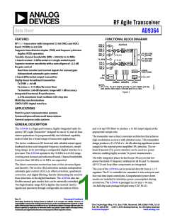
Functional Block Diagram .............................................................. 1
General Description......................................................................... 1
Revision History ............................................................................... 2
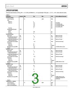
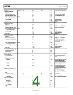
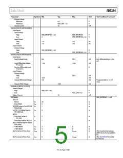
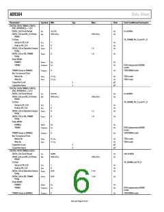
Specifications..................................................................................... 3
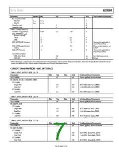
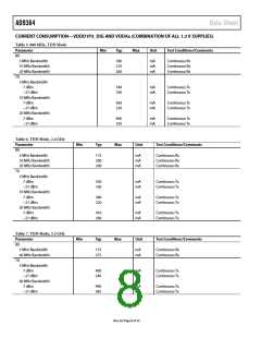
Current Consumption—VDD_Interface.................................. 7
Current Consumption—VDDD1P3_DIG and VDDAx
(Combination of All 1.3 V Supplies) ......................................... 8
Absolute Maximum Ratings ..................................................... 10
Reflow Profile.............................................................................. 10
Thermal Resistance .................................................................... 10
ESD Caution................................................................................ 10
Pin Configuration and Function Descriptions........................... 11
Typical Performance Characteristics ........................................... 15
800 MHz Frequency Band......................................................... 15
2.4 GHz Frequency Band .......................................................... 20
REVISION HISTORY
2/14—Revision B: Initial Version
Rev. B | Page 2 of 32

 ADI [ ADI ]