Data Sheet
AD9364
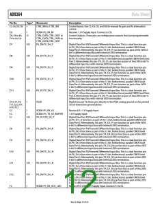
Pin No.
Type1 Mnemonic
I/O P0_D10/TX_D5_N
Description
F8
Digital Data Port P0/Transmit Differential Input Bus. This is a dual function pin.
As P0_D10, it functions as part of the 12-bit, bidirectional, parallel CMOS level
Data Port 0. Alternatively, this pin (TX_D5_N) can function as part of the LVDS
6-bit Tx differential input bus with internal LVDS termination.
F10, G10
I
FB_CLK_P, FB_CLK_N
Feedback Clock. These pins receive the FB_CLK signal that clocks in Tx data. In
CMOS mode, use FB_CLK_P as the input and tie FB_CLK_N to ground.
F12
G1
G2
I
I
O
VDDD1P3_DIG
RX_EXT_LO_IN
RX_VCO_LDO_OUT
1.3 V Digital Supply Input.
External Receive LO Input. When this pin is unused, tie it to ground.
Receive VCO LDO Output. Connect this pin directly to G3 and a 1 μF bypass
capacitor in series with a 1 Ω resistor to ground.
G3
G5
I
I
VDDA1P1_RX_VCO
EN_AGC
Receive VCO Supply Input. Connect this pin directly to G2 only.
Manual Control Input for Automatic Gain Control (AGC).
G6
I
ENABLE
Control Input. This pin moves the device through various operational states.
G7, G8
O
RX_FRAME_N, RX_FRAME_P
Receive Digital Data Framing Output Signal. These pins transmit the RX_FRAME
signal that indicates whether the Rx output data is valid. In CMOS mode, use
RX_FRAME_P as the output and leave RX_FRAME_N unconnected.
G9, H9
G11, H11
H1, J1
I
TX_FRAME_P, TX_FRAME_N
DATA_CLK_P, DATA_CLK_N
RXB_P, RXB_N
Transmit Digital Data Framing Input Signal. These pins receive the TX_FRAME
signal that indicates when Tx data is valid. In CMOS mode, use TX_FRAME_P as
the input and tie TX_FRAME_N to ground.
Receive Data Clock Output. These pins transmit the DATA_CLK signal that is used
by the BBP to clock Rx data. In CMOS mode, use DATA_CLK_P as the output and
leave DATA_CLK_N unconnected.
Receive Channel Differential Input B. Alternatively, each pin can be used as a
single-ended input. These inputs experience degraded performance above
3 GHz. Unused pins must be tied to ground.
O
I
H4
H5
H8
I
TXNRX
Enable State Machine Control Signal. This pin controls the data port bus direction.
Logic low selects the Rx direction; logic high selects the Tx direction.
Input to Synchronize Digital Clocks Between Multiple AD9364 Devices. If this pin
is unused, it must be tied to ground.
Digital Data Port P1/Receive Differential Output Bus. This is a dual function pin.
As P1_D11, it functions as part of the 12-bit bidirectional parallel CMOS level
Data Port 1. Alternatively, this pin (RX_D5_P) can function as part of the LVDS
6-bit Rx differential output bus with internal LVDS termination.
I
SYNC_IN
I/O
P1_D11/RX_D5_P
H12
J3
J4
I
I
I
I
VDD_INTERFACE
VDDA1P3_RX_SYNTH
SPI_DI
1.2 V to 2.5 V Supply for Digital I/O Pins (1.8 V to 2.5 V in LVDS Mode).
1.3 V Supply Input.
SPI Serial Data Input.
SPI Clock Input.
J5
SPI_CLK
J6
O
CLK_OUT
Output Clock. This pin can be configured to output either a buffered version of the
external input clock, the DCXO, or a divided-down version of the internal ADC_CLK.
J7
I/O
I/O
I/O
I/O
I/O
P1_D10/RX_D5_N
P1_D9/RX_D4_P
P1_D7/RX_D3_P
P1_D5/RX_D2_P
P1_D3/RX_D1_P
Digital Data Port P1/Receive Differential Output Bus. This is a dual function pin.
As P1_D10, it functions as part of the 12-bit bidirectional parallel CMOS level
Data Port 1. Alternatively, this pin (RX_D5_N) can function as part of the LVDS
6-bit Rx differential output bus with internal LVDS termination.
Digital Data Port P1/Receive Differential Output Bus. This is a dual function pin.
As P1_D9, it functions as part of the 12-bit bidirectional parallel CMOS level
Data Port 1. Alternatively, this pin (RX_D4_P) can function as part of the LVDS
6-bit Rx differential output bus with internal LVDS termination.
Digital Data Port P1/Receive Differential Output Bus. This is a dual function pin.
As P1_D7, it functions as part of the 12-bit bidirectional parallel CMOS level
Data Port 1. Alternatively, this pin (RX_D3_P) can function as part of the LVDS
6-bit Rx differential output bus with internal LVDS termination.
Digital Data Port P1/Receive Differential Output Bus. This is a dual function pin.
As P1_D5, it functions as part of the 12-bit bidirectional parallel CMOS level
Data Port 1. Alternatively, this pin (RX_D2_P) can function as part of the LVDS
6-bit Rx differential output bus with internal LVDS termination.
J8
J9
J10
J11
Digital Data Port P1/Receive Differential Output Bus. This is a dual function pin.
As P1_D3, it functions as part of the 12-bit bidirectional parallel CMOS level
Data Port 1. Alternatively, this pin (RX_D1_P) can function as part of the LVDS
6-bit Rx differential output bus with internal LVDS termination.
Rev. B | Page 13 of 32

 ADI [ ADI ]