AD9268
AD9268BCPZ-80
AD9268BCPZ-105
AD9268BCPZ-125
Parameter1
Temp
Min
Typ
Max
Min
Typ
Max
Min Typ
Max
Unit
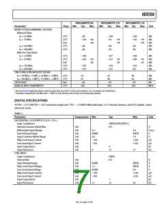
WORST OTHER (HARMONIC OR SPUR)
Without Dither
fIN = 2.4 MHz
fIN = ꢁ± MHz
2ꢀ°C
2ꢀ°C
Full
2ꢀ°C
2ꢀ°C
−99
−1±± −96
−96
−98
−96
−1±±
−99
−1±±
−1±± −94
−94
−98
−96
dBc
dBc
dBc
dBc
dBc
−94
−94
fIN = 14± MHz
fIN = 2±± MHz
−98
−94
With On-Chip Dither
fIN = 2.4 MHz
fIN = ꢁ± MHz
2ꢀ°C
2ꢀ°C
Full
2ꢀ°C
2ꢀ°C
−1±8
−1±6 −96
−96
−1±ꢀ
−1±2
−1±ꢁ
−1±ꢁ −9ꢀ
−9ꢀ
−1±4
−1±2
−1±8
−1±6 −9ꢀ
−9ꢀ
−1±3
−99
dBc
dBc
dBc
dBc
dBc
fIN = 14± MHz
fIN = 2±± MHz
TWO-TONE SFDR, WITHOUT DITHER
fIN = 29 MHz (−ꢁ dBFS ), 32 MHz (−ꢁ dBFS)
fIN = 169 MHz (−ꢁ dBFS ), 1ꢁ2 MHz (−ꢁ dBFS)
CROSSTALK2
2ꢀ°C
2ꢀ°C
Full
93
81
92
8±
9±
82
dBc
dBc
dB
−9ꢀ
6ꢀ±
−9ꢀ
6ꢀ±
−9ꢀ
6ꢀ±
ANALOG INPUT BANDWIDTH
2ꢀ°C
MHz
1 See the AN-83ꢀ Application Note, Understanding High Speed ADC Testing and Evaluation, for a complete set of definitions.
2 Crosstalk is measured at 1±± MHz with −1 dBFS on one channel and no input on the alternate channel.
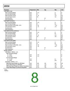
DIGITAL SPECIFICATIONS
AVDD = 1.8 V, DRVDD = 1.8 V, maximum sample rate, VIN = −1.0 dBFS differential input, 1.0 V internal reference, and DCS enabled, unless
otherwise noted.
Table 3.
Parameter
Temperature Min
Typ
Max
Unit
DIFFERENTIAL CLOCK INPUTS (CLK+, CLK−)
Logic Compliance
CMOS/LVDS/LVPECL
±.9
Internal Common-Mode Bias
Differential Input Voltage
Input Voltage Range
Input Common-Mode Range
High Level Input Current
Low Level Input Current
Input Capacitance
Full
V
Full
Full
Full
Full
Full
Full
Full
±.3
AGND
±.9
−1±±
−1±±
3.6
AVDD
1.4
V p-p
V
V
+1±±
+1±±
μA
μA
pF
kΩ
4
1±
Input Resistance
8
12
SYNC INPUT
Logic Compliance
Internal Bias
CMOS
±.9
Full
Full
Full
Full
Full
Full
Full
Full
V
Input Voltage Range
High Level Input Voltage
Low Level Input Voltage
High Level Input Current
Low Level Input Current
Input Capacitance
AGND
1.2
AGND
−1±±
−1±±
AVDD
AVDD
±.6
V
V
V
+1±±
+1±±
μA
μA
pF
kΩ
1
16
Input Resistance
12
2±
Rev. A | Page ꢁ of 44

 ADI [ ADI ]