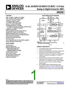
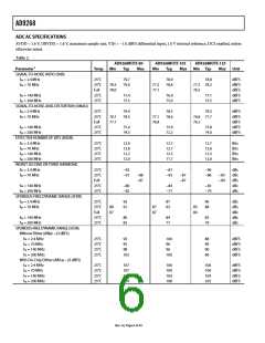
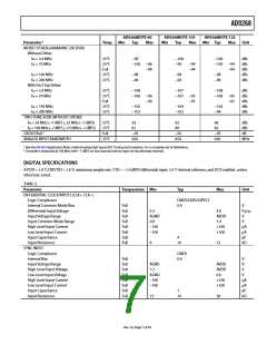
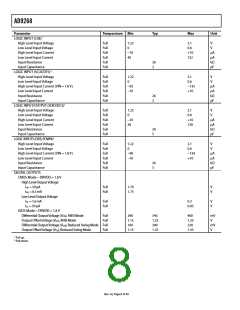
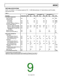
AD9268
AD9268BCPZ-80
Temperature Min Typ Max Min Typ
AD9268BCPZ-105
AD9268BCPZ-125
Max
Parameter
Max Min Typ
Unit
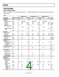
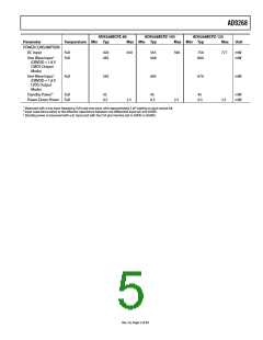
POWER CONSUMPTION
DC Input
Sine Wave Input1
(DRVDD = 1.8 V
CMOS Output
Mode)
Full
Full
42±
48ꢀ
4ꢀ±
ꢀ6ꢀ
6±8
ꢀ9±
ꢁꢀ±
8±±
ꢁꢁꢁ
mW
mW
Sine Wave Input1
(DRVDD = 1.8 V
LVDS Output
Mode)
Full
ꢀ82
68ꢀ
8ꢁ±
mW
Standby Power3
Full
4ꢀ
±.ꢀ
4ꢀ
±.ꢀ
4ꢀ
±.ꢀ
mW
mW
Power-Down Power Full
2.ꢀ
2.ꢀ
2.ꢀ
1 Measured with a low input frequency, full-scale sine wave, with approximately ꢀ pF loading on each output bit.
2 Input capacitance refers to the effective capacitance between one differential input pin and AGND.
3 Standby power is measured with a dc input and with the CLK pins inactive (set to AVDD or AGND).
Rev. A | Page ꢀ of 44

 ADI [ ADI ]