AD9268
TABLE OF CONTENTS
Features .............................................................................................. 1
Clock Input Considerations...................................................... 30
Channel/Chip Synchronization................................................ 31
Power Dissipation and Standby Mode .................................... 32
Digital Outputs ........................................................................... 32
Timing ......................................................................................... 33
Built-In Self-Test (BIST) and Output Test .................................. 34
Built-In Self-Test (BIST)............................................................ 34
Output Test Modes..................................................................... 34
Serial Port Interface (SPI).............................................................. 35
Configuration Using the SPI..................................................... 35
Hardware Interface..................................................................... 36
Configuration Without the SPI ................................................ 36
SPI Accessible Features.............................................................. 36
Memory Map .................................................................................. 37
Reading the Memory Map Register Table............................... 37
Memory Map Register Table..................................................... 38
Memory Map Register Descriptions........................................ 40
Applications Information.............................................................. 41
Design Guidelines ...................................................................... 41
Outline Dimensions....................................................................... 42
Ordering Guide .......................................................................... 42
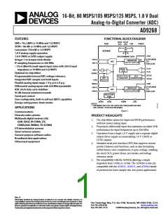
Applications....................................................................................... 1
Functional Block Diagram .............................................................. 1
Product Highlights ........................................................................... 1
Revision History ............................................................................... 2
General Description......................................................................... 3
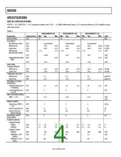
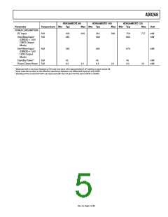
Specifications..................................................................................... 4
ADC DC Specifications............................................................... 4
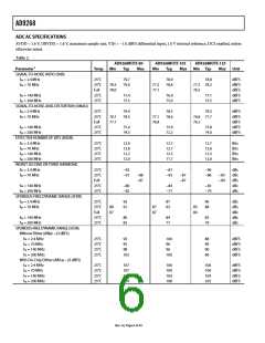
ADC AC Specifications ................................................................. 6
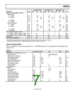
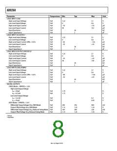
Digital Specifications ................................................................... 7
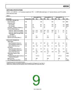
Switching Specifications ................................................................ 9
Timing Specifications ................................................................ 10
Absolute Maximum Ratings.......................................................... 12
Thermal Characteristics ............................................................ 12
ESD Caution................................................................................ 12
Pin Configurations and Function Descriptions ......................... 13
Typical Performance Characteristics ........................................... 17
Equivalent Circuits......................................................................... 25
Theory of Operation ...................................................................... 26
ADC Architecture ...................................................................... 26
Analog Input Considerations.................................................... 26
Voltage Reference ....................................................................... 29
REVISION HISTORY
9/09—Rev. 0 to Rev. A
Changes to Features List.................................................................. 1
Changes to Specifications Section.................................................. 4
Changes to Table 5.......................................................................... 10
Changes to Typical Performance Characteristics Section......... 17
5/09—Revision 0: Initial Version
Rev. A | Page 2 of 44

 ADI [ ADI ]