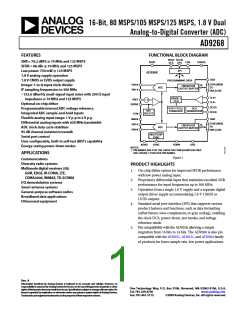
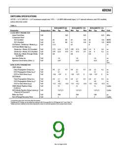
AD9268
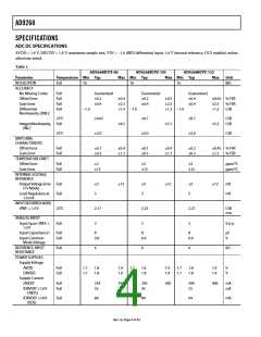
SPECIFICATIONS
ADC DC SPECIFICATIONS
AVDD = 1.8 V, DRVDD = 1.8 V, maximum sample rate, VIN = −1.0 dBFS differential input, 1.0 V internal reference, DCS enabled, unless
otherwise noted.
Table 1.
AD9268BCPZ-80
Temperature Min Typ
AD9268BCPZ-105
Max Min Typ Max Min Typ
16 16
AD9268BCPZ-125
Parameter
Max
Unit
RESOLUTION
ACCURACY
Full
16
Bits
No Missing Codes
Offset Error
Gain Error
Full
Full
Full
Full
Guaranteed
±±.2
±±.4
Guaranteed
±±.2
±±.4
Guaranteed
±±.4
±±.4
±±.4
±2.ꢀ
+1.4 −1.±
±±.ꢀ
±2.ꢀ
+1.3 −1.±
±±.6ꢀ % FSR
±2.ꢀ
+1.2
% FSR
LSB
Differential
−1.±
Nonlinearity (DNL)1
2ꢀ°C
±±.6ꢀ
±2.±
±±.ꢁ
±3.±
±±.ꢁ
±3.±
LSB
LSB
Integral Nonlinearity Full
(INL)1
±4.ꢀ
±ꢀ.1
±ꢀ.ꢀ
2ꢀ°C
LSB
MATCHING
CHARACTERISTIC
Offset Error
Gain Error
Full
Full
±±.1
±±.3
±±.4
±1.3
±±.1
±±.3
±±.4
±1.3
±±.2
±±.3
±±.4ꢀ % FSR
±1.3
% FSR
TEMPERATURE DRIFT
Offset Error
Gain Error
Full
Full
±2
±1ꢀ
±2
±1ꢀ
±2
±1ꢀ
ppm/°C
ppm/°C
INTERNAL VOLTAGE
REFERENCE
Output Voltage Error Full
(1 V Mode)
±ꢀ
ꢀ
±12
±ꢀ
ꢀ
±12
±ꢀ
ꢀ
±12
mV
mV
Load Regulation @
1.± mA
Full
INPUT REFERRED NOISE
VREF = 1.± V
2ꢀ°C
Full
2.1ꢁ
2
2.23
2
2.2ꢁ
2
LSB
rms
ANALOG INPUT
Input Span, VREF =
1.± V
Input Capacitance2
Input Common-
Mode Voltage
V p-p
Full
Full
8
±.9
8
±.9
8
±.9
pF
V
REFERENCE INPUT
RESISTANCE
Full
6
6
6
kΩ
POWER SUPPLIES
Supply Voltage
AVDD
Full
Full
1.ꢁ
1.ꢁ
1.8
1.8
1.9
1.9
1.ꢁ
1.ꢁ
1.8
1.8
1.9
1.9
1.ꢁ
1.ꢁ
1.8
1.8
1.9
1.9
V
V
DRVDD
Supply Current
IAVDD1
IDRVDD1 (1.8 V
CMOS)
Full
Full
234
3ꢀ
24±
293
4ꢀ
3±±
39±
ꢀꢀ
4±±
mA
mA
IDRVDD1 (1.8 V
LVDS)
Full
89
89
94
mA
Rev. A | Page 4 of 44

 ADI [ ADI ]