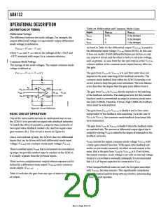
AD8132
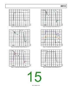
V
= ±5V
S
G = +1
V
S
= 3V
V
= 2V p-p
O, dm
R
= 499Ω
L, dm
2mV
10
5ns
300mV
5ns
0
5
15
20
25
30
35
40
5ns/DIV
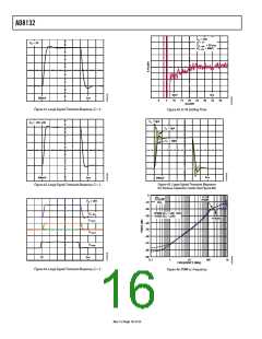
Figure 41. Large Signal Transient Response, G = 2
Figure 44. 0.1% Settling Time
C
= 0pF
L
V
S
= +5V, ±5V
C
= 5pF
L
C
= 20pF
L
5ns
400mV
5ns
400mV
Figure 45. Large Signal Transient Response
for Various Capacitor Loads (See Figure 60)
Figure 42. Large Signal Transient Response, G = 2
0
–10
–20
–30
ΔV
O, dm
–PSRR
V
= ±5V
O, dm
S
ΔV
S
+PSRR (V = ±5V, +5V)
S
–PSRR (V = ±5V)
V
S
+PSRR
V
–OUT
–40
–50
V
+OUT
–60
–70
–80
–90
V
+DIN
1V
5ns
0.1
1
10
FREQUENCY (MHz)
100
1k
Figure 43. Large Signal Transient Response, G = 2
Figure 46. PSRR vs. Frequency
Rev. F | Page 16 of 32

 ADI [ ADI ]