AD7714
ABSOLUTE MAXIMUM RATINGS*
(TA = +25°C unless otherwise noted)
SOIC Package, Power Dissipation . . . . . . . . . . . . . . . . 450 mW
θJA Thermal Impedance . . . . . . . . . . . . . . . . . . . . . . 75°C/W
Lead Temperature, Soldering
Vapor Phase (60 sec) . . . . . . . . . . . . . . . . . . . . . . +215°C
Infrared (15 sec) . . . . . . . . . . . . . . . . . . . . . . . . . . +220°C
SSOP Package, Power Dissipation . . . . . . . . . . . . . . . . 450 mW
θJA Thermal Impedance . . . . . . . . . . . . . . . . . . . . . 109°C/W
Lead Temperature, Soldering
Vapor Phase (60 sec) . . . . . . . . . . . . . . . . . . . . . . +215°C
Infrared (15 sec) . . . . . . . . . . . . . . . . . . . . . . . . . . +220°C
TSSOP Package, Power Dissipation . . . . . . . . . . . . . . 450 mW
θJA Thermal Impedance . . . . . . . . . . . . . . . . . . . . . 128°C/W
Lead Temperature, Soldering
AVDD to AGND . . . . . . . . . . . . . . . . . . . . . . . . –0.3 V to +7 V
AVDD to DGND . . . . . . . . . . . . . . . . . . . . . . . . –0.3 V to +7 V
DVDD to AGND . . . . . . . . . . . . . . . . . . . . . . . . –0.3 V to +7 V
DVDD to DGND . . . . . . . . . . . . . . . . . . . . . . . . –0.3 V to +7 V
Analog Input Voltage to AGND . . . . . –0.3 V to AVDD + 0.3 V
Reference Input Voltage to AGND . . . –0.3 V to AVDD + 0.3 V
Digital Input Voltage to DGND . . . . . –0.3 V to DVDD + 0.3 V
Digital Output Voltage to DGND . . . . –0.3 V to DVDD + 0.3 V
Operating Temperature Range
Commercial (A Version) . . . . . . . . . . . . . . . –40°C to +85°C
Extended (Y Version) . . . . . . . . . . . . . . . . . –40°C to +105°C
Storage Temperature Range . . . . . . . . . . . . . –65°C to +150°C
Junction Temperature . . . . . . . . . . . . . . . . . . . . . . . . . .+150°C
Plastic DIP Package, Power Dissipation . . . . . . . . . . . 450 mW
θJA Thermal Impedance . . . . . . . . . . . . . . . . . . . . . 105°C/W
Lead Temperature (Soldering, 10 sec) . . . . . . . . . . . .+260°C
Vapor Phase (60 sec) . . . . . . . . . . . . . . . . . . . . . . +215°C
Infrared (15 sec) . . . . . . . . . . . . . . . . . . . . . . . . . . +220°C
*Stresses above those listed under Absolute Maximum Ratings may cause perma-
nent damage to the device. This is a stress rating only; functional operation of the
device at these or any other conditions above those listed in the operational
sections of this specification is not implied. Exposure to absolute maximum rating
conditions for extended periods may affect device reliability.
CAUTION
ESD (electrostatic discharge) sensitive device. Electrostatic charges as high as 4000 V readily
accumulate on the human body and test equipment and can discharge without detection.
Although these devices feature proprietary ESD protection circuitry, permanent damage may still
occur on these devices if they are subjected to high energy electrostatic discharges. Therefore,
proper ESD precautions are recommended to avoid performance degradation or loss of functionality.
WARNING!
ESD SENSITIVE DEVICE
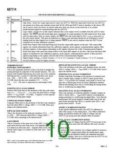
PIN CONFIGURATIONS
SSOP
DIP and SOIC/TSSOP
SCLK
DGND
DV
SCLK
MCLK IN
DGND
DV
DD
MCLK IN
MCLK OUT
POL
DIN
MCLK OUT
POL
DD
DOUT
DIN
DOUT
DRDY
CS
SYNC
SYNC
RESET
AIN1
DRDY
CS
RESET
NC
AD7714
TOP VIEW
AD7714
TOP VIEW
NC
AGND
AIN6
NC
NC
(Not to Scale)
(Not to Scale)
AIN2
AGND
AIN6
AIN1
AIN2
AIN3
AIN5
AIN4
REF IN(+)
REF IN(–)
BUFFER
AIN3
AIN4
AIN5
REF IN(+)
REF IN(–)
BUFFER
STANDBY
AV
DD
STANDBY
AV
DD
NC = NO CONNECT
–8–
REV. C

 ADI [ ADI ]