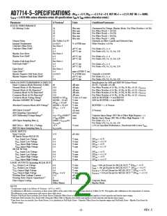
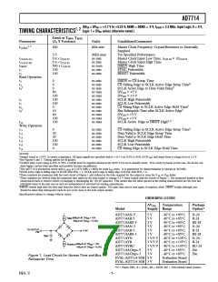
AD7714–SPECIFICATIONS (AVDD = + 3.3 V to +5 V, DVDD = +3.3 V to +5 V, REF IN(+) = +1.25 V (AD7714-3) or +2.5 V
(AD7714-5); REF IN(–) = AGND; MCLK IN = 1 MHz to 2.4576 MHz unless otherwise noted. All specifications TMIN to TMAX unless otherwise noted.)
Parameter
A Versions
Units
Conditions/Comments
TRANSDUCER BURNOUT14
Current
Initial Tolerance
Drift
1
±10
0.1
µA nom
% typ
%/°C typ
SYSTEM CALIBRATION
Positive Full-Scale Calibration Limit15
(1.05 × VREF)/GAIN
V max
GAIN Is the Selected PGA Gain (Between 1 and 128)
GAIN Is the Selected PGA Gain (Between 1 and 128)
GAIN Is the Selected PGA Gain (Between 1 and 128)
GAIN Is the Selected PGA Gain (Between 1 and 128)
GAIN Is the Selected PGA Gain (Between 1 and 128)
Negative Full-Scale Calibration Limit15 –(1.05 × VREF)/GAIN V max
Offset Calibration Limit16
Input Span16
–(1.05 × VREF)/GAIN V max
0.8 × VREF/GAIN
(2.1 × VREF)/GAIN
V min
V max
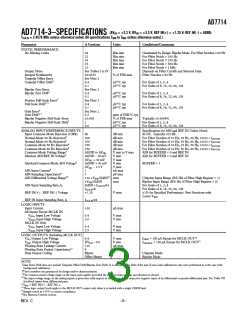
POWER REQUIREMENTS
Power Supply Voltages
AVDD Voltage (AD7714-3)
AVDD Voltage (AD7714-5)
DVDD Voltage
+3 to +3.6
+4.75 to +5.25
+3 to +5.25
V
V
V
For Specified Performance
For Specified Performance
For Specified Performance
Power Supply Currents
AVDD Current
AVDD = 3.3 V or 5 V. BST Bit of Filter High Register = 017
Typically 0.2 mA. BUFFER = 0 V. fCLK IN = 1 MHz or 2.4576 MHz
Typically 0.4 mA. BUFFER = DVDD. fCLK IN = 1 MHz or 2.4576 MHz
AVDD = 3.3 V or 5 V. BST Bit of Filter High Register = 117
Typically 0.3 mA. BUFFER = 0 V. fCLK IN = 2.4576 MHz
Typically 0.8 mA. BUFFER = DVDD. fCLK IN = 2.4576 MHz
Digital I/Ps = 0 V or DVDD. External MCLK IN
0.27
0.6
mA max
mA max
0.5
1.1
mA max
mA max
DVDD Current18
0.23
0.4
0.5
0.8
mA max
mA max
mA max
mA max
dB typ
Typically 0.15 mA. DVDD = 3.3 V. fCLK IN = 1 MHz
Typically 0.3 mA. DVDD = 5 V. fCLK IN = 1 MHz
Typically 0.4 mA. DVDD = 3.3 V. fCLK IN = 2.4576 MHz
Typically 0.6 mA. DVDD = 5 V. fCLK IN = 2.4576 MHz
Power Supply Rejection19
See Note 20
Normal-Mode Power Dissipation18
AVDD = DVDD = +3.3 V. Digital I/Ps = 0 V or DVDD. External MCLK IN
Typically 1.25 mW. BUFFER = 0 V. fCLK IN = 1 MHz. BST Bit = 0
Typically 1.8 mW. BUFFER = +3.3 V. fCLK IN = 1 MHz. BST Bit = 0
Typically 2 mW. BUFFER = 0 V. fCLK IN = 2.4576 MHz. BST Bit = 0
Typically 2.6 mW. BUFFER = +3.3 V. fCLK IN = 2.4576 MHz. BST Bit = 0
AVDD = DVDD = +5 V. Digital I/Ps = 0 V or DVDD. External MCLK IN
Typically 2.5 mW. BUFFER = 0 V. fCLK IN = 1 MHz. BST Bit = 0
Typically 3.5 mW. BUFFER = +5 V. fCLK IN = 1 MHz. BST Bit = 0
Typically 4 mW. BUFFER = 0 V. fCLK IN = 2.4576 MHz. BST Bit = 0
Typically 5 mW. BUFFER = +5 V. fCLK IN = 2.4576 MHz. BST Bit = 0
External MCLK IN = 0 V or DVDD. Typically 20 µA. VDD = +5 V
External MCLK IN = 0 V or DVDD. Typically 5 µA. VDD = +3.3 V
1.65
2.75
2.55
3.65
mW max
mW max
mW max
mW max
Normal-Mode Power Dissipation
3.35
5
5.35
7
40
10
mW max
mW max
mW max
mW max
µA max
Standby (Power-Down) Current21
Standby (Power-Down) Current21
µA max
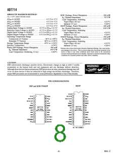
NOTES
15After calibration, if the input voltage exceeds positive full scale, the converter will output all 1s. If the input is less than negative full scale, then the device outputs all 0s.
16These calibration and span limits apply provided the absolute voltage on the analog inputs does not exceed AVDD + 30 mV or go more negative than AGND – 30 mV. The
offset calibration limit applies to both the unipolar zero point and the bipolar zero point.
17For higher gains (≥8) at fCLK IN = 2.4576 MHz, the BST bit of the Filter High Register must be set to 1. For other conditions, it can be set to 0.
18When using a crystal or ceramic resonator across the MCLK pins as the clock source for the device, the DVDD current and power dissipation will vary depending on the crystal
or resonator type (see Clocking and Oscillator Circuit section).
19Measured at dc and applies in the selected passband. PSRR at 50 Hz will exceed 120 dB with filter notches of 5 Hz, 10 Hz, 25 Hz or 50 Hz. PSRR at 60 Hz will exceed 120 dB
with filter notches of 6 Hz, 10 Hz, 30 Hz or 60 Hz.
20PSRR depends on gain. For Gain of 1 : 70 dB typ: For Gain of 2 : 75 dB typ; For Gain of 4 : 80 dB typ; For Gains of 8 to 128 : 85 dB typ.
21If the external master clock continues to run in standby mode, the standby current increases to 150 µA typical with 5 V supplies and 75 µA typical with 3.3 V supplies. When
using a crystal or ceramic resonator across the MCLK pins as the clock source for the device, the internal oscillator continues to run in standby mode and the power dissipation
depends on the crystal or resonator type (see Standby Mode section).
Specifications subject to change without notice.
–4–
REV. C

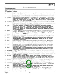
 ADI [ ADI ]