AD7714
AD7714-5 OUTPUT NOISE
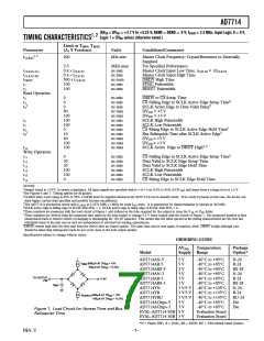
Table Ia shows the output rms noise and effective resolution for some typical notch and –3 dB frequencies for the AD7714-5 with
fCLK IN = 2.4576 MHz while Table Ib gives the information for fCLK IN = 1 MHz. The numbers given are for the bipolar input ranges
with a VREF of +2.5 V and with BUFFER = 0. These numbers are typical and are generated at an analog input voltage of 0 V. The
numbers in brackets in each table are for the effective resolution of the part (rounded to the nearest 0.5 LSB). The effective resolu-
tion of the device is defined as the ratio of the output rms noise to the input full scale (i.e., 2 × VREF/GAIN). It should be noted that
it is not calculated using peak-to-peak output noise numbers. Peak-to-peak noise numbers can be up to 6.6 times the rms numbers
while effective resolution numbers based on peak-to-peak noise can be 2.5 bits below the effective resolution based on rms noise as
quoted in the tables.
2
The output noise from the part comes from two sources. The first is the electrical noise in the semiconductor devices used in the
implementation of the modulator (device noise). Secondly, when the analog input signal is converted into the digital domain, quan-
tization noise is added. The device noise is at a low level and is largely independent of frequency. The quantization noise starts at
an even lower level but rises rapidly with increasing frequency to become the dominant noise source. Consequently, lower filter
notch settings (below 100 Hz approximately for fCLK IN = 2.4576 MHz and below 40 Hz approximately for fCLK IN = 1 MHz) tend to
be device noise dominated while higher notch settings are dominated by quantization noise. Changing the filter notch and cutoff
frequency in the quantization-noise dominated region results in a more dramatic improvement in noise performance than it does in
the device-noise dominated region as shown in Table I. Furthermore, quantization noise is added after the PGA, so effective resolu-
tion is largely independent of gain for the higher filter notch frequencies. Meanwhile, device noise is added in the PGA and, there-
fore, effective resolution reduces at high gains for lower notch frequencies. Additionally, in the device-noise dominated region, the
output noise (in µV) is largely independent of reference voltage while in the quantization-noise dominated region, the noise is pro-
portional to the value of the reference. It is possible to do post-filtering on the device to improve the output data rate for a given
–3 dB frequency and also to further reduce the output noise.
At the lower filter notch settings (below 60 Hz for fCLK IN = 2.4576 MHz and below 25 Hz for fCLK IN = 1 MHz), the no missing
codes performance of the device is at the 24-bit level. At the higher settings, more codes will be missed until at 1 kHz notch setting
for fCLK IN = 2.4576 MHz (400 Hz for fCLK IN = 1 MHz), no missing codes performance is only guaranteed to the 12-bit level.
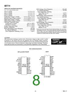
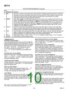
Table Ia. AD7714-5 Output Noise/Resolution vs. Gain and First Notch for fCLK IN = 2.4576 MHz, BUFFER = 0
Typical Output RMS Noise in V (Effective Resolution in Bits)
Filter First
Notch & O/P –3 dB
Gain of
1
Gain of
2
Gain of
4
Gain of
8
Gain of
16
Gain of
32
Gain of
64
Gain of
128
Data Rate
Frequency
5 Hz
1.31 Hz
2.62 Hz
6.55 Hz
7.86 Hz
13.1 Hz
15.72 Hz
26.2 Hz
65.5 Hz
131 Hz
262 Hz
0.87 (22.5) 0.48 (22.5) 0.24 (22.5) 0.2 (21.5) 0.18 (20.5) 0.17 (20) 0.17 (19) 0.17 (18)
10 Hz
25 Hz
30 Hz
50 Hz
60 Hz
100 Hz
250 Hz
500 Hz
1 kHz
1.0
1.8
2.5
4.33 (20)
5.28 (20)
12.1 (18.5) 5.9
127 (15.5) 58
(22.5) 0.78 (21.5) 0.48 (21.5) 0.33 (21) 0.25 (20.5) 0.25 (19.5) 0.25 (18.5) 0.25 (17.5)
(21.5) 1.1 (21) 0.63 (21) 0.5 (20) 0.44 (19.5) 0.41 (18.5) 0.38 (17.5) 0.38 (16.5)
0.84 (20.5) 0.57 (20) 0.46 (19.5) 0.43 (18.5) 0.4 (17.5) 0.4 (16.5)
(21)
1.31 (21)
2.06 (20)
2.36 (20)
1.2 (20)
1.33 (20)
(18.5) 2.86 (19)
0.64 (20) 0.54 (19)
0.87 (19.5) 0.63 (19)
1.91 (18.5) 1.06 (18)
0.46 (18.5) 0.46 (17.5) 0.46 (16.5)
0.62 (18) 0.6 (17) 0.56 (16)
0.83 (17.5) 0.82 (16.5) 0.76 (15.5)
(15.5) 29 (15.5) 15.9 (15.5) 6.7 (15.5) 3.72 (15.5) 1.96 (15.5) 1.5 (14.5)
533 (13)
2,850 (11)
267 (13)
1,258 (11)
137 (13)
680 (11)
66 (13) 38 (13)
297 (11) 131 (11)
20 (13) 8.6 (13) 4.4 (13)
99 (10.5) 53 (10.5) 28 (10.5)
Table Ib. AD7714-5 Output Noise/Resolution vs. Gain and First Notch for fCLK IN = 1 MHz, BUFFER = 0
Typical Output RMS Noise in V (Effective Resolution in Bits)
Filter First
Notch & O/P –3 dB
Gain of
1
Gain of
2
Gain of
4
Gain of
8
Gain of
16
Gain of
32
Gain of
64
Gain of
128
Data Rate
Frequency
2 Hz
4 Hz
0.52 Hz
1.05 Hz
2.62 Hz
6.55 Hz
7.86 Hz
13.1 Hz
15.72 Hz
26.2 Hz
52.4 Hz
104.8 Hz
0.75 (22.5) 0.56 (22)
1.04 (22)
1.66 (21.5) 1.01 (21.5) 0.77 (20.5) 0.41 (20.5) 0.37 (19.5) 0.35 (19) 0.35 (18) 0.35 (17)
0.31 (22)
0.19 (21.5) 0.17 (21)
0.14 (20) 0.14 (19) 0.14 (18)
0.88 (21.5) 0.45 (21.5) 0.28 (21) 0.21 (20.5) 0.21 (19.5) 0.21 (18.5) 0.21 (17.5)
10 Hz
25 Hz
30 Hz
50 Hz
60 Hz
100 Hz
200 Hz
400 Hz
5.2
7.1
19.4 (18)
(20)
(19.5) 3.28 (19.5) 1.42 (19.5) 1.07 (19) 0.78 (18.5) 0.64 (18) 0.61 (17) 0.61 (16)
9.11 (18) 4.2 (18) 2.45 (18) 1.56 (17.5) 1.1 (17) 0.82 (16.5) 0.8 (15.5)
(17.5) 16
2.06 (20)
1.4 (20)
0.86 (19.5) 0.63 (19)
0.61 (18) 0.59 (17) 0.59 (16)
25
(17.5) 6.5 (17.5) 2.9 (17.5) 1.93 (17.5) 1.4 (17) 1.1 (16) 0.98 (15.5)
(15.5) 25 (15.5) 13.5 (15.5) 5.7 (15.5) 3.9 (15.5) 2.1 (15) 1.3 (15)
102 (15.5) 58
637 (13)
2,830 (11)
259 (13)
1,430 (11)
130 (13)
720 (11)
76 (13) 33 (13)
334 (11) 220 (10.5) 94 (10.5) 54 (10.5) 25 (10.5)
16 (13) 11 (13)
6
(12.5)
REV. C
–11–

 ADI [ ADI ]