AD7714
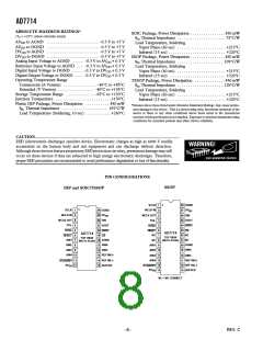
PIN FUNCTION DESCRIPTION
DIP/SOIC PIN NUMBERS
Pin
No. Mnemonic
Function
1
SCLK
Serial Clock. Logic Input. An external serial clock is applied to this input to access serial data from the
AD7714. This serial clock can be a continuous clock with all data transmitted in a continuous train of pulses.
Alternatively, it can be a noncontinuous clock with the information being transmitted to the AD7714 in smaller
batches of data.
2
2
MCLK IN
Master Clock signal for the device. This can be provided in the form of a crystal/resonator or external clock. A
crystal/resonator can be tied across the MCLK IN and MCLK OUT pins. Alternatively, the MCLK IN pin can
be driven with a CMOS-compatible clock and MCLK OUT left unconnected. The part is specified with clock
input frequencies of both 1 MHz and 2.4576 MHz.
3
4
MCLK OUT When the master clock for the device is a crystal/resonator, the crystal/resonator is connected between MCLK
IN and MCLK OUT. If an external clock is applied to the MCLK IN, MCLK OUT provides an inverted clock
signal. This clock can be used to provide a clock source for external circuits.
POL
Clock Polarity. Logic Input. With this input low, the first transition of the serial clock in a data transfer
operation is from a low to a high. In microcontroller applications, this means that the serial clock should idle
low between data transfers. With this input high, the first transition of the serial clock in a data transfer
operation is from a high to a low. In microcontroller applications, this means that the serial clock should idle
high between data transfers.
5
SYNC
Logic Input which allows for synchronization of the digital filters and analog modulators when using a number
of AD7714s. While SYNC is low, the nodes of the digital filter, the filter control logic and the calibration
control logic are reset and the analog modulator is also held in its reset state. SYNC does not affect the digital
interface and does not reset DRDY if it is low.
6
7
RESET
Logic Input. Active low input which resets the control logic, interface logic, digital filter and analog modulator
of the part to power-on status.
Analog Input Channel 1. Programmable-gain analog input which can be used as a pseudo-differential input
when used with AIN6 or as the positive input of a differential analog input pair when used with AIN2 (see
Communications Register section).
AIN1
8
9
AIN2
AIN3
Analog Input Channel 2. Programmable-gain analog input which can be used as a pseudo-differential input
when used with AIN6 or as the negative input of a differential analog input pair when used with AIN1 (see
Communications Register section).
Analog Input Channel 3. Programmable-gain analog input which can be used as a pseudo-differential input
when used with AIN6 or as the positive input of a differential analog input pair when used with AIN4 (see
Communications Register section).
10 AIN4
Analog Input Channel 4. Programmable-gain analog input which can be used as a pseudo-differential input
when used with AIN6 or as the negative input of a differential analog input pair when used with AIN3 (see
Communications Register section).
11 STANDBY
Logic Input. Taking this pin low shuts down the analog and digital circuitry, reducing current consumption to
typically 5 µA.
12 AVDD
Analog Positive Supply Voltage, A Grade Versions: +3.3 V nominal (AD7714-3) or +5 V nominal (AD7714-5);
Y Grade Versions: 3 V or 5 V nominal.
13 BUFFER
Buffer Option Select. Logic Input. With this input low, the on-chip buffer on the analog input (after the
multiplexer and before the analog modulator) is shorted out. With the buffer shorted out the current flowing in
the AVDD line is reduced to 270 µA. With this input high, the on-chip buffer is in series with the analog input
allowing the inputs to handle higher source impedances.
14 REF IN(–)
15 REF IN(+)
Reference Input. Negative input of the differential reference input to the AD7714. The REF IN(–) can lie
anywhere between AVDD and AGND provided REF IN(+) is greater than REF IN(–).
Reference Input. Positive input of the differential reference input to the AD7714. The reference input is
differential with the provision that REF IN(+) must be greater than REF IN(–). REF IN(+) can lie anywhere
between AVDD and AGND.
16 AIN5
17 AIN6
18 AGND
Analog Input Channel 5. Programmable-gain analog input which is the positive input of a differential analog
input pair when used with AIN6 (see Communications Register section).
Analog Input Channel 6. Reference point for AIN1 through AIN4 in pseudo-differential mode or as the
negative input of a differential input pair when used with AIN5 (see Communications Register section).
Ground reference point for analog circuitry.
REV. C
–9–

 ADI [ ADI ]