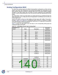
Device Architecture
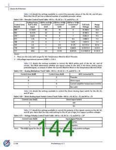
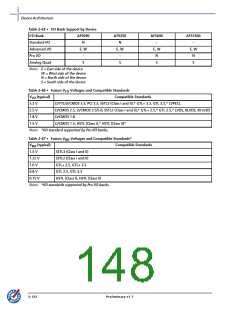
Table 2-54 details the settings available to control the prescaler values of the AV, AC, and AT pins.
Note that the AT pin has a reduced number of available prescaler values.
Table 2-54 • Prescaler Control Truth Table—AV (x = 0), AC (x = 1), and AT (x = 3)
Scaling Factor, LSB for an 8-Bit LSB for a 10-Bit LSB for a 12-Bit
Control Lines
Bx[2:0]
Pad to ADC
Input
Conversion2
(mV)
Conversion2
(mV)
Conversion2
(mV)
Full-Scale
Voltage
Range
Name
000 1
0.15625
0.3125
0.625
1.25
64
32
16
8
16
8
4
2
16.368 V
8.184 V
16 V
8 V
001
010 1
011
4
1
4.092 V
4 V
2
0.5
2.046 V
2 V
100
2.5
4
1
0.25
0.125
0.0625
0.03125
1.023 V
1 V
101
5.0
2
0.5
0.25
0.125
0.5115 V
0.25575 V
0.127875 V
0.5 V
0.25 V
0.125 V
110
10.0
1
111
20.0
0.5
Notes:
1. These are the only valid ranges for the Temperature Monitor Block Prescaler.
2. LSB voltage equivalences assume VAREF = 2.56 V.
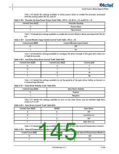
Table 2-55 details the settings available to control the MUX within each of the AV, AC, and AT
circuits. This MUX determines whether the signal routed to the ADC is the direct analog input,
prescaled signal, or output of either the Current Monitor Block or the Temperature Monitor Block.
Table 2-55 • Analog Multiplexer Truth Table—AV (x = 0), AC (x = 1), and AT (x = 3)
Control Lines Bx[4]
Control Lines Bx[3]
ADC Connected To
0
0
1
1
0
1
0
1
Prescaler
Direct input
Current amplifier temperature monitor
Not valid
Table 2-56 details the settings available to control the Direct Analog Input switch for the AV, AC,
and AT pins.
Table 2-56 • Direct Analog Input Switch Control Truth Table—AV (x = 0), AC (x = 1), and AT (x = 3)
Control Lines Bx[5]
Direct Input Switch
0
1
Off
On
Table 2-57 details the settings available to control the polarity of the signals coming to the AV, AC,
and AT pins. Note that the only valid setting for the AT pin is logic 0 to support positive voltages.
Table 2-57 • Voltage Polarity Control Truth Table—AV (x = 0), AC (x = 1), and AT (x = 3)*
Control Lines Bx[6]
Input Signal Polarity
Positive
0
1
Negative
Note: *The B3[6] signal for the AT pad should be kept at logic 0 to accept only positive voltages.
2-128
Preliminary v1.7

 ACTEL [ Actel Corporation ]