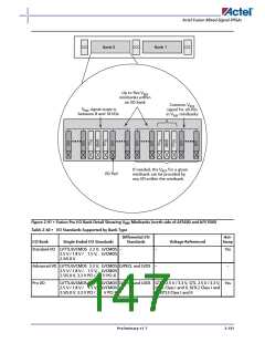
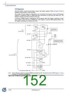
Device Architecture
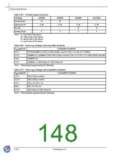
Table 2-65 • I/O Bank Support by Device
I/O Bank
AFS090
AFS250
AFS600
AFS1500
Standard I/O
Advanced I/O
Pro I/O
N
E, W
–
N
E, W
–
–
E, W
N
–
E, W
N
Analog Quad
S
S
S
S
Note: E = East side of the device
W = West side of the device
N = North side of the device
S = South side of the device
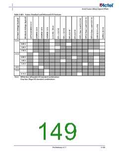
Table 2-66 • Fusion VCCI Voltages and Compatible Standards
CCI (typical) Compatible Standards
LVTTL/LVCMOS 3.3, PCI 3.3, SSTL3 (Class I and II),* GTL+ 3.3, GTL 3.3,* LVPECL
V
3.3 V
2.5 V
1.8 V
1.5 V
LVCMOS 2.5, LVCMOS 2.5/5.0, SSTL2 (Class I and II),* GTL+ 2.5,* GTL 2.5,* LVDS, BLVDS, M-LVDS
LVCMOS 1.8
LVCMOS 1.5, HSTL (Class I),* HSTL (Class II)*
Note: *I/O standard supported by Pro I/O banks.
Table 2-67 • Fusion VREF Voltages and Compatible Standards*
VREF (typical)
Compatible Standards
1.5 V
1.25 V
1.0 V
0.8 V
0.75 V
SSTL3 (Class I and II)
SSTL2 (Class I and II)
GTL+ 2.5, GTL+ 3.3
GTL 2.5, GTL 3.3
HSTL (Class I), HSTL (Class II)
Note: *I/O standards supported by Pro I/O banks.
2-132
Preliminary v1.7

 ACTEL [ Actel Corporation ]