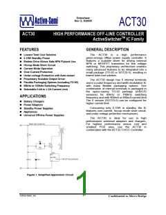
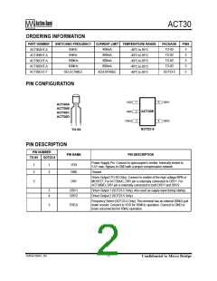
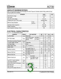
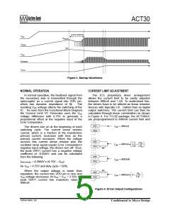
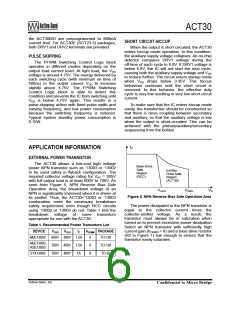
ACT30
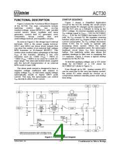
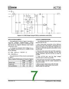
Figure 6. A 3.75W Charger Using ACT30A in combination with ACT32
APPLICATION EXAMPLE
LAYOUT CONSIDERATIONS
The application circuit in Figure 6 provides a
5V/0.75A constant voltage/constant current
output. An ACT30A is used in combination with
the ACT32 for highest efficiency and lowest
component count.
The following should be observed when doing
layout for the ACT30:
1. Use a "star point" connection at the GND pin
of ACT30 for the VDD bypass components (C5
and C6 in Figure 6), the input filter capacitor (C2
in Figure 6) and other ground connections on the
primary side.
To change the constant output voltage VOUTCV
and constant current limit IOUTCC, modify R7 and
R6 as following:
2. Keep the loop across the input filter capacitor,
the transformer primary windings, and the high
voltage transistor, and the ACT30 as small as
possible.
R7 = 80kΩ • [(VOUTCV - 1V)/3.8V - 1]
R6 = 250mV/IOUTCC
The performance of this circuit is summarized
in Table 2.
Table 2. System Performance of Circuit in Figure 6
3. Keep ACT30 pins and the high voltage
transistor pins as short as possible.
4. Keep the loop across the secondary windings,
the output diode, and the output capacitors as
small as possible.
110VAC
0.09W
0.75A
65%
220VAC
0.15W
0.75A
67%
Standby Power
Current Limit
Full Load Efficiency
5. Allow enough copper area under the high
voltage transistor, output diode, and current
shunt resistor for heat sink.
Active-Semi, Inc.
- 7 -
Confidential to Micro Bridge

 ACT [ ADVANCED CRYSTAL TECHNOLOGY ]