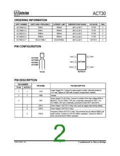
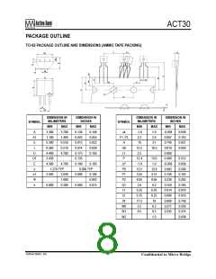
ACT30
the ACT30B/D are preprogrammed to 800mA
current limit. For ACT30E (SOT23-5) packages,
both DRV1 and DRV2 terminals are provided.
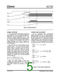
SHORT CIRCUIT HICCUP
When the output is short circuited, the ACT30
enters hiccup mode operation. In this condition,
the auxiliary supply voltage collapses. An on-chip
detector compares DRV1 voltage during the
off-time of each cycle to 6.8V. If DRV1 voltage is
below 6.8V, the IC will not start the next cycle,
causing both the auxiliary supply voltage and VDD
to reduce further. The circuit enters startup mode
when VDD drops below 3.35V. This hiccup
behaviour continues until the short circuit is
removed. In this behavior, the effective duty
cycle is very low resulting in very low short circuit
current.
PULSE SKIPPING
The PFWM Switching Control Logic block
operates in different modes depending on the
output load current level. At light load, the VDD
voltage is around 4.75V. The energy delivered by
each switching cycle (with minimum on time of
500ns) to the output causes VDD to increase
slightly above 4.75V. The FPWM Switching
Control Logic block is able to detect this
condition and prevents the IC from switching until
VDD is below 4.75V again. This results in a
pulse-skipping action with fixed pulse width and
varying frequency, and low power consumption
because the switching frequency is reduced.
Typical system standby power consumption is
0.15W.
To make sure that the IC enters hiccup mode
easily, the transformer should be constructed so
that there is close coupling between secondary
and auxiliary, so that the auxiliary voltage is low
when the output is short-circuited. This can be
achieved with the primary/auxiliary/secondary
sequencing from the bobbin.
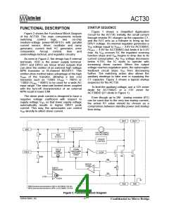
IC
APPLICATION INFORMATION
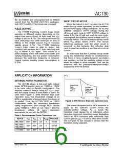
EXTERNAL POWER TRANSISTOR
The ACT30 allows a low-cost high voltage
power NPN transistor such as ‘13003 or ‘13002
to be used safely in flyback configuration. The
required collector voltage rating for VAC = 265V
with full output load is at least 600V to 700V. As
seen from Figure 5, NPN Reverse Bias Safe
Operation Area, the breakdown voltage of an
NPN is significantly improved when it is driven at
its emitter. Thus, the ACT30+’13002 or ‘13003
combination meet the necessary breakdown
safety requirement even though RCC circuits
using ‘13002 or ‘13003 do not. Table 1 lists the
breakdown voltage of some transistors
appropriate for use with the ACT30.
Base-Drive
Safe
Emitter-
Drive Safe
Region
Region
(RCC)
(ACT30)
VC
Figure 5. NPN Reverse Bias Safe Operation Area
The power dissipated in the NPN transistor is
equal to the collector current times the
collector-emitter voltage. As
a
result, the
transistor must always be in saturation when
turned on to prevent excessive power dissipation.
Select an NPN transistor with sufficiently high
current gain (hFEMIN > 8) and a base drive resistor
(R2 in Figure 1) low enough to ensure that the
transistor easily saturates.
Table 1. Recommended Power Transistors List
DEVICE
VCBO
VCEO
IC
hFEMIN PACKAGE
MJE13002
600V 300V 1.5A
8
8
8
TO-126
TO-126
TO-92
MJE13003,
700V 400V 1.5A
KSE13003
STX13003
700V 400V
1A
Active-Semi, Inc.
- 6 -
Confidential to Micro Bridge

 ACT [ ADVANCED CRYSTAL TECHNOLOGY ]