ACT30
ABSOLUTE MAXIMUM RATINGS
(Note: Do not exceed these limits to prevent damage to the device. Exposure to absolute maximum rating conditions for long
periods may affect device reliability.)
PARAMETER
VALUE
-0.3 to 6
20
UNIT
V
mA
V
VDD, FREQ Pin Voltage
VDD Current
DRV, DRV1, DRV2 Voltage
-0.3 to 18
Internally limited
0.6
Continuous DRV, DRV1, DRV2 Current
A
TO-92
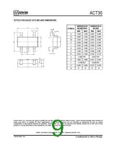
SOT23-5
Maximum Power Dissipation
W
0.39
Operating Junction Temperature
Storage Temperature
Lead Temperature (Soldering, 10 sec)
-40 to 150
-55 to 150
300
°C
°C
°C
ELECTRICAL CHARACTERISTICS
(VDD = 4V, TJ = 25°C unless otherwise specified)
PARAMETER
VDD Start Voltage
SYMBOL
TEST CONDITIONS
MIN
TYP
5
8.6
MAX
5.25
10.5
UNIT
VSTART
Rising edge
4.75
V
DRV1 must be higher ACT30A/C
DRV1 Start Voltage
VDRVST
V
than this voltage to
ACT30B/D
9.6
11.5
start up.
DRV1 Short-Circuit Detect Threshold
VDD Under-voltage Threshold
VDD Clamp Voltage
Startup Supply Current
Supply Current
VSCDRV
VUV
6.8
3.35
5.45
0.23
0.7
V
V
V
mA
mA
Falling edge
10mA
VDD = 4V before VUV
3.17
5.15
3.53
5.75
0.45
1
IDDST
IDD
ACT30A/B or FREQ = 0
55
75
67
60
65
100
75
85
125
83
Switching Frequency
fSW
kHz
ACT30C/D or FREQ = VDD
ACT30A/C, VDD = 4V
ACT30B/D, VDD = 4V
VDD = 4.6V
Maximum Duty Cycle
Minimum Duty Cycle
DMAX
DMIN
%
%
3.5
ACT30A/C
ACT30B/D; ACT30E
with DRV1 = DRV2
400
VDD = VUV
0.1V
+
Effective Current Limit
ILIM
mA
800
VDD to DRV1 Current Coefficient
VDD Dynamic Impedance
DRV1 or DRV2 Driver On-Resistance
DRV1 Rise Time
GGAIN
RVDD
-0.29
9
3.6
30
A/V
kΩ
Ω
RDRV1, 2 IDRV1 = IDRV2 = 0.05A
1nF load, 15Ω pull-up
ns
ns
DRV1 Fall Time
1nF load, 15Ω pull-up
20
DRV1 and DRV2 Switch Off Current
Driver off, VDRV1 = VDRV2 = 10V
12
30
µA
Active-Semi, Inc.
- 3 -
Confidential to Micro Bridge

 ACT [ ADVANCED CRYSTAL TECHNOLOGY ]