ACT30
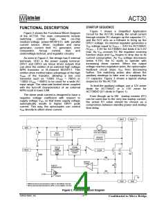
STARTUP SEQUENCE
FUNCTIONAL DESCRIPTION
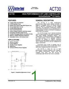
Figure 1 shows a Simplified Application
Circuit for the ACT30. Initially, the small current
through resistor R1 charges up the capacitor C1,
and the BJT acts as a follower to bring up the
DRV1 voltage. An internal regulator generates a
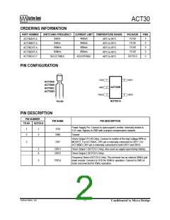
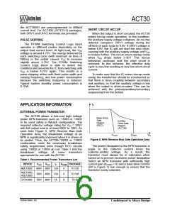
Figure 2 shows the Functional Block Diagram
of the ACT30. The main components include
switching
control
logic,
two
on-chip
medium-voltage power-MOSFETs with parallel
current sensor, driver, oscillator and ramp
generator, current limit VC generator, error
V
DD voltage equal to VDRV1 – 3.6V for ACT30A/C
(VDRV1 – 4.6V for ACT30B/D) but limits it to 5.5V
max. As VDD crosses 5V, the regulator sourcing
function stops and VDD begins to drop due to its
current consumption. As VDD voltage decreases
below 4.75V, the IC starts to operate with
increasing driver current. When the output
voltage reaches regulation point, the optocoupler
feedback circuit stops VDD from decreasing
further. The switching action also allows the
auxiliary windings to take over in supplying the
C1 capacitor. Figure 3 shows a typical startup
sequence for the ACT30.
comparator,
hiccup
control,
bias
and
undervoltage-lockout, and regulator circuitry.
As seen in Figure 2, the design has 6 internal
terminals. VDD is the power supply terminal.
DRV1 and DRV2 are linear driver outputs that
can drive the emitter of an external high voltage
NPN transistor or N-channel MOSFET. This
emitter-drive method takes advantage of the high
VCBO of the transitor, allowing a low cost
transistor such as ‘13003 (VCBO = 700V) or
‘13002 (VCBO = 600V) to be used for a wide AC
input range. The slew-rate limited driver coupled
with the turn-off characteristics of an external
NPN result in lower EMI.
To limit the auxiliary voltage, use a 12V zener
diode for ACT30A/C or a 13V zener for
ACT30B/D (D1 diode in Figure 1).
The driver peak current is designed to have a
negative voltage coefficient with respect to
supply voltage VDD, so that lower supply voltage
automatically results in higher DRV1 peak
current. This way, the optocoupler can control
Even though up to 2Mꢀ startup resistor (R1)
can be used due to the very low startup current,
the actual R1 value should be chosen as a
compromise between standby power and startup
time delay.
VDD directly to affect driver current.
DRV1
DRV2 ‡
REGULATOR
− +
VDD
3.6V (ACT30A/C)
4.6V (ACT30B/D)
9k
BIAS
& UVLO
HICCUP
CONTROL
OSC &
PFWM
SWITCHING
CONTROL
LOGIC
FREQ †
RAMP
CURRENT
SLEW
1x
40
56x
56x
200k
20k
ERROR
COMP
+
−
ILIM VC
GENERATOR
20k
−
4.75V
+
10uA/V
GND
GND
† FREQ terminal wire-bonded to VDD in ACT30C/D (TO-92)
‡ DRV2 terminal wire-bonded to DRV1 in ACT30B/D (TO-92)
Figure 2. Functional Block Diagram
Active-Semi, Inc.
- 4 -
Confidential to Micro Bridge

 ACT [ ADVANCED CRYSTAL TECHNOLOGY ]