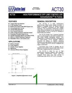
ACT30
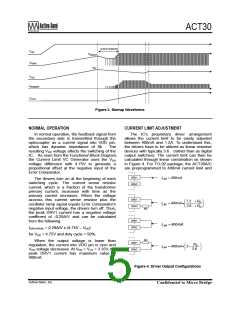
pulse-skipped
VAC
VDRVST
VDRV1
5V
VDD
IPRIMARY
VOUT
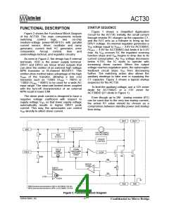
Figure 3. Startup Waveforms
NORMAL OPERATION
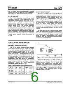
CURRENT LIMIT ADJUSTMENT
In normal operation, the feedback signal from
the secondary side is transmitted through the
optocoupler as a current signal into VDD pin,
which has dynamic impedance of 9kꢀ. The
resulting VDD voltage affects the switching of the
IC. As seen from the Functional Block Diagram,
the Current Limit VC Generator uses the VDD
voltage difference with 4.75V to generate a
proportional offset at the negative input of the
Error Comparator.
The IC's proprietary driver arrangement
allows the current limit to be easily adjusted
between 400mA and 1.2A. To understand this,
the drivers have to be utilized as linear resistive
devices with typically 3.6ꢀ (rather than as digital
output switches). The current limit can then be
calculated through linear combination as shown
in Figure 4. For TO-92 package, the ACT30A/C
are preprogrammed to 400mA current limit and
DRV1
ILIM = 400mA
The drivers turn on at the beginning of each
switching cycle. The current sense resistor
current, which is a fraction of the transformer
primary current, increases with time as the
primary current increases. When the voltage
accross this current sense resistor plus the
oscillator ramp signal equals Error Comparator's
negative input voltage, the drivers turn off. Thus,
the peak DRV1 current has a negative voltage
coefficent of -0.29A/V and can be calculated
from the following:
DRV2
DRV1
7.2ꢀ + RD
3.6ꢀ + RD
ILIM = 400mA•
ILIM = 800mA
DRV2
RD
DRV1
DRV2
IDRV1PEAK = 0.29A/V • (4.75V – VDD
)
for VDD < 4.75V and duty cycle < 50%.
RD
When the output voltage is lower than
regulation, the current into VDD pin is zero and
VDD voltage decreases. At VDD = VUV = 3.35V, the
peak DRV1 current has maximum value of
400mA.
DRV1
DRV2
RD
3.6ꢀ
ILIM = 400mA• 2 +
Figure 4. Driver Output Configurations
Active-Semi, Inc.
- 5 -
Confidential to Micro Bridge

 ACT [ ADVANCED CRYSTAL TECHNOLOGY ]