FEDL87V2107-01
OKI Semiconductor
ML87V2107
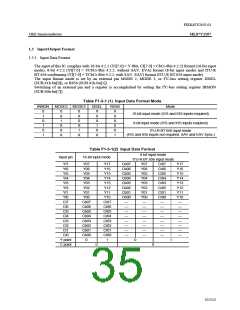
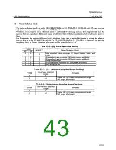
The data and control signal interfaces according to output system modes are as follows.
• 16-bit output mode
Vertical Sync. signal:
Horizontal Sync. signal:
Data output pin:
OVS
OHS
YO[7:0], CI[7:0] (YCbCr-4:2:2)
Output system clock frequency:
Clip level:
f
OCLK = 12.2727272/13.5/14.31818/14.75 MHz
None
* The crystal is used with 24.545454/27/28.63636/29.5MHz in 16-bit output mode also.
(The clock of 12.2727272/13.5/14.31818/14.75MHz which is divided by 2 internally is output from the OCLK
pin.)
• 8-bit output mode
Vertical Sync. signal:
Horizontal Sync. signal:
Data output pin:
Output system clock frequency:
Clip level:
OVS
OHS
YO[7:0], (YCbCr-4:2:2) * CO[7:0] is Hi-Z.
fOCLK = 24.545454/27/28.63636/29.5 MHz
None
* Cannot be used in external synchronous mode (INT = 0, ASYNC = 0) that does not use internal Sync. signal
generation function.
• ITU-R BT.656 output mode
Vertical Sync. signal:
Horizontal Sync. signal:
Data output pin:
Output system clock frequency:
Clip level:
SAV, EAV split
SAV, EAV split
YI[7:0] (YCbCr-4:2:2)
fOCLK = 27 MHz
00h R 01h, FFh R FEh
* Cannot be used in external synchronous mode (INT = 0, ASYNC = 0) that does not use internal Sync. signal
generation function.
* The V signals that are contained in SAV and EAV comply with ITU-R BT.656-4.
* Sync. signals equivalent to those in 8-bit output mode are output from OVS and OHS.
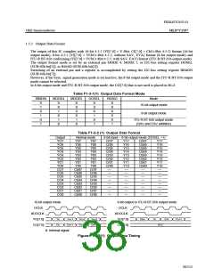
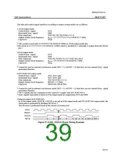
• Internal output clock (OOCLK)
In 16-bit output mode, OOCLK = OCLK is set and in 8-bit output mode and ITU-R BT.656 output mode, the
clock pulse is generated by dividing OCLK by 2.
This division is performed based on the release of system reset.
OCLK
RESET
OOCLK
Cn
Yn
Cn+1
Yn+1
YI[7:0]
Figure F1-3-2(2) OOCLK Phase Timing Example
39/152

 OKI [ OKI ELECTRONIC COMPONETS ]