FEDL87V2107-01
OKI Semiconductor
ML87V2107
1.2 Output Memory Control
This IC reads data from the frame memory by generating a line a memory control signal from the Sync. signal of
the OVS and OHS pin inputs or Sync. signal from the internal Sync. signal generator.
1.2.1 Output Control Mode Settings
In the output control mode, six modes, shown Table F1-1-1 (2), can be selected by setting either the external
setting pin mode (IRMON = 0 (SUB:40h-bit [7]) or internal register mode (IRMON = 1).
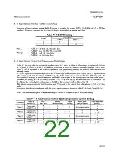
Table F1-2-1(1) Output Control Mode Setting Allocation
VMD
HMD
IRMON
[1]
[0]
[1]
[0]
MODE0
(External pin)
SUB:40h-bit[0]
MODE1
(External pin)
SUB:40h-bit[2]
0
1
SUB:40h-bit[1]
SUB:40h-bit[1]
SUB:40h-bit[3]
SUB:40h-bit[3]
Table F1-2-1(2) Output Control Mode Settings
VMD
HMD
Standard clock
frequency fOCLK
[MHz]
Number of
valid lines
Standard
pixels per line
Vertical mode
Valid pixels
[1]
[0]
[1]
[0]
0
0
0
0
1
0
0
0
0
0
0
1
625/50Hz 2:1
525/60Hz 2:1
625/50Hz 2:1
288(304)
243(254)
288(304)
13.5/27
864
858
944
720
720
768
13.5/27
14.75/29.5
12.272727/
24.545454
14.75/29.5
14.31818/
28.63636
0
0
0
1
0
1
0
1
1
1
0
0
525/60Hz 2:1
625/50Hz 2:1
525/60Hz 2:1
243(254)
288(304)
243(254)
780
944
910
640
768
768
Others
Test modes (not settable)
*: ( ) indicates only ITU-RBT.656 input/output mode can be selected.
26/152

 OKI [ OKI ELECTRONIC COMPONETS ]