¡ Semiconductor
MSM5412222
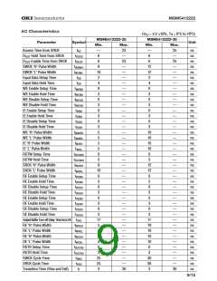
AC Characteristics
(VCC = 5 V 10ꢀ, Ta = 0°C to 70°C)
MSM5412222-25
MSM5412222-30
Unit
Parameter
Symbol
Min.
—
6
Max.
23
—
23
—
—
—
—
—
—
—
—
—
—
—
—
—
—
—
—
—
—
—
—
—
—
—
—
—
—
—
—
—
—
—
—
—
—
—
—
—
30
Min.
—
6
Max.
25
—
25
—
—
—
—
—
—
—
—
—
—
—
—
—
—
—
—
—
—
—
—
—
—
—
—
—
—
—
—
—
—
—
—
—
—
—
—
—
30
Access Time from SRCK
tAC
tDDCK
tDECK
tWSWH
tWSWL
tDS
ns
ns
ns
ns
ns
ns
ns
ns
ns
ns
ns
ns
ns
ns
ns
ns
ns
ns
ns
ns
ns
ns
ns
ns
ns
ns
ns
ns
ns
ns
ns
ns
ns
ns
ns
ns
ns
ns
ns
ns
ns
D
D
OUT Hold Time from SRCK
OUT Enable Time from SRCK
6
6
SWCK "H" Pulse Width
SWCK "L" Pulse Width
Input Data Setup Time
Input Data Hold Time
WE Enable Setup Time
WE Enable Hold Time
WE Disable Setup Time
WE Disable Hold Time
IE Enable Setup Time
IE Enable Hold Time
IE Disable Setup Time
IE Disable Hold Time
WE "H" Pulse Width
WE "L" Pulse Width
IE "H" Pulse Width
9
12
12
2
10
2
tDH
4
4
tWENS
tWENH
tWDSS
tWDSH
tIENS
0
0
3
3
0
0
3
3
0
0
tIENH
3
3
tIDSS
0
0
tIDSH
3
3
tWWEH
tWWEL
tWIEH
tWIEL
tRSTWS
tRSTWH
tWSRH
tWSRL
tRENS
tRENH
tRDSS
tRDSH
tOENS
tOENH
tODSS
tODSH
5
10
10
10
10
0
5
5
IE "L" Pulse Width
5
RSTW Setup Time
0
RSTW Hold Time
3
3
SRCK "H" Pulse Width
SRCK "L" Pulse Width
RE Enable Setup Time
RE Enable Hold Time
RE Disable Setup Time
RE Disable Hold Time
OE Enable Setup Time
OE Enable Hold Time
OE Disable Setup Time
OE Disable Hold Time
9
12
12
0
10
0
3
3
0
0
3
3
0
0
3
3
0
0
3
3
Output Buffer Turn-off Delay Time from OE tOEZ
17
5
17
10
10
10
10
0
RE "H" Pulse Width
RE "L" Pulse Width
OE "H" Pulse Width
OE "L" Pulse Width
RSTR Setup Time
RSTR Hold Time
tWREH
tWREL
tWOEH
tWOEL
tRSTRS
tRSTRH
tSWC
5
5
5
0
3
3
SWCK Cycle Time
SRCK Cycle Time
25
25
3
30
30
3
tSRC
Transition Time (Rise and Fall)
tT
9/15

 OKI [ OKI ELECTRONIC COMPONETS ]