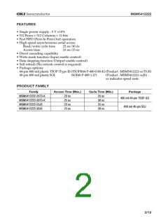
¡ Semiconductor
MSM5412222
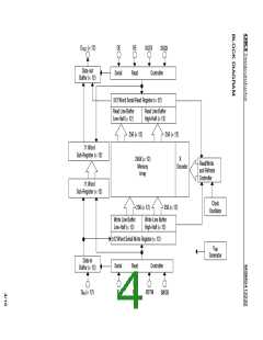
Read Operation
The read operation is controlled by three clocks, SRCK, RSTR, and RE. Read operation is
accomplished by cycling SRCK, and holding RE high after the read address pointer reset
operation or RSTR.
Each read operation, which begins after RSTR, must contain at least 80 active read cycles, i.e.
SRCK cycles while RE is high.
Read Reset : RSTR
The first positive transition of SRCK after RSTR becomes high resets the read address counters
to zero. RSTR setup and hold times are referenced to the rising edge of SRCK. Because the read
reset function is solely controlled by the SRCK rising edge after the high level of RSTR, the states
of RE and OE are ignored in the read reset cycle.
Before RSTR may be brought high again for a further reset operation, it must be low for at least
*two SRCK cycles.
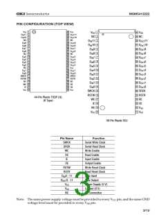
Data Out : D
0 - 11
OUT
Read Clock : SRCK
Data is shifted out of the data registers. It is triggered by the rising edge of SRCK when RE is high
during a read operation. The SRCK input increments the internal read address pointer when RE
is high.
The three-state output buffer provides direct TTL compatibility ( no pullup resistor required).
Data out is the same polarity as data in. The output becomes valid after the access time interval
t
AC
that begins with the rising edge of SRCK. *There are no output valid time restriction on
MSM5412222.
Read Enable : RE
The function of RE is to gate of the SRCK clock for incrementing the read pointer. When RE is
high before the rising edge of SRCK, the read pointer is incremented. When RE is low, the read
pointer is not incremented. RE setup times (t
and t
) and RE hold times (t
and
RENS
RDSS
RENH
t
) are referenced to the rising edge of the SRCK clock.
RDSH
Output Enable : OE
OE is used to enable/disable the outputs. OE high level enables the outputs. The internal read
address pointer is always incremented by cycling SRCK regardless of the OE level. Note that OE
setup and hold times are referenced to the rising edge of SRCK.
6/15

 OKI [ OKI ELECTRONIC COMPONETS ]