Absolute Maximum Ratings (Note 1)
Soldering Information, Lead Temperature
QSOP Package (Note 3)
Vapor Phase (60 seconds)
Infrared (15 seconds)
Supply Voltage
−0.3V to 6.0V
215˚C
220˚C
Voltage at Any Pin:
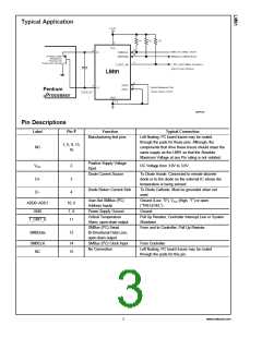
NC (Pins 1,5,9), ADD0, ADD1, D+
−0.3V to
(VCC + 0.3V)
−0.3V to 6.0V
ESD Susceptibility (Note 4)
Human Body Model
2500V
250V
All other pins (except D−)
D− Input Current
Machine Model
±
1 mA
Input Current at All Other Pins (Note
2)
5 mA
Operating Ratings
Package Input Current (Note 2)
SMBData, T_CRIT_A Output Sink
Current
20 mA
(Note 1) and (Note 5)
Specified Temperature Range
LM91D
TMIN to TMAX
0˚C to +125˚C
+3.0V to +3.6V
10 mA
6.0V
Output Voltage
Supply Voltage Range (VCC
)
Storage Temperature
−65˚C to +150˚C
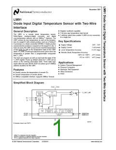
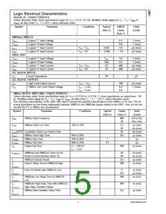
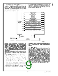
Temperature-to-Digital Converter Characteristics
Unless otherwise noted, these specifications apply for VCC=+3.0 Vdc to +3.6 Vdc. Boldface limits apply for TA = TJ = TMIN
to TMAX; all other limits TA= TJ=+25˚C, unless otherwise noted.
Typical
LM91D
Limits
Units
Parameter
Conditions
(Note 6)
(Note 7)
(Limit)
±
Local Temperature Error (Note 8)
Remote Temperature Error using Pentium Diode
(Note 8) and (Note 9)
1
˚C
±
±
+60˚C ≤TA ≤ +100˚C,
VCC = 3.3 Vdc
4
6
˚C (max)
˚C (max)
0˚C ≤ TA ≤ +125˚C,
VCC = 3.3 Vdc
Remote Temperature Error using Diode
Connected 2N3904 (Note 8) and (Note 9)
+60˚C ≤TA ≤ +100˚C,
VCC = 3.3 Vdc
+2, −6
+4, −8
˚C (max)
˚C (max)
0˚C ≤ TA ≤ +125˚C,
VCC = 3.3 Vdc
Resolution
8
Bits
˚C
1
Temperature Conversion Time
Quiescent Current (Note 10)
D− Source Voltage
(Note 11)
SMBus (I2C Inactive)
120
0.500
0.7
145
1
ms
mA (max)
V
Diode Source Current
(D+ − D−)=+ 0.65V; high
level
160
50
µA (max)
µA (min)
µA (max)
µA (min)
V (max)
V (max)
V (min)
Low level
16
5
T_CRIT_A Output Saturation Voltage
Power-On Reset Threshold
IOUT = 3.0 mA
0.4
2.2
1.2
On VCC input, falling edge
www.national.com
4

 OKI [ OKI ELECTRONIC COMPONETS ]