EM785830AA
8-bit Micro-controller
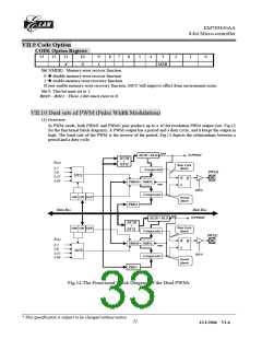
VII.9 Code Option
CODE Option Register
13
12
11
10
9
8
7
6
5
4
3
2
1
0
0
0
1
MER
Bit 3(MER) : Memory error recover function
0 Î disable memory error recover function
1 Î enable memory error recovery function
If user enable memory error recovery function, MCU will improve effect from environment noise.
Bit 9: This bit must set to 1.
Bit10 ~ Bit11 : These 2 bits must clear to 0.
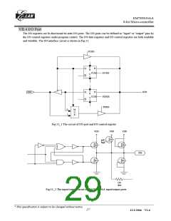
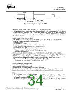
VII.10 Dual sets of PWM (Pulse Width Modulation)
(1) Overview
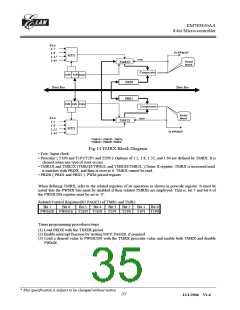
In PWM mode, both PWM1 and PWM2 pins produce up to a 10-bit resolution PWM output (see. Fig.12
for the functional block diagram). A PWM output has a period and a duty cycle, and it keeps the output in
high. The baud rate of the PWM is the inverse of the period. Fig.13 depicts the relationships between a
period and a duty cycle.
latch
To PWM1IF
DL2H + DL2L
DT2H
+
Fosc
DT2L
Duty Cycle
Match
1:2
1:8
1:32
1:64
Comparator
PWM1
MUX
R
S
Q
TMR1H + TMR1L
reset
IOC6
Comparator
T1P0 T1P1 T1EN
Period
Match
PRD1
Data Bus
Data Bus
latch
To PWM2IF
DL2H + DL2L
DT2H
+
DT2L
Duty Cycle
Match
T2P0 T2P1 T2EN
Comparator
PWM2
Fosc
R
S
Q
TMR2H + TMR2L
1:2
1:8
1:32
1:64
reset
MUX
IOC6
Comparator
Period
Match
PRD2
Fig.12 The Functional Block Diagram of the Dual PWMs
__________________________________________________________________________________________________________________________________________________________________
* This specification is subject to be changed without notice.
31
12/1/2004 V1.6

 ELAN [ ELAN MICROELECTRONICS CORP ]