EM785830AA
8-bit Micro-controller
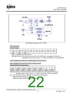
Bit 7: Unused register. Always keep this bit to 0 or some un-expect error will happen!
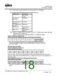
The status after wake-up and the wake-up sources list as the table below.
Wakeup signal
SLEEP mode
RA(7,6)=(0,0)
+ SLEP
TCC time out
IOCF bit0=1
No function
COUNTER1 time out No function
IOCF bit1=1
COUNTER2 time out No function
IOCF bit2=2
WDT time out
Reset and jump to
address 0
PORT7 (0,3)
Reset and Jump to
address 0
<Note> PORT70 's wakeup function is controlled by IOCF bit 3. It's falling edge or rising edge trigger
(controlled by CONT register bit7).
PORT73 's wakeup function is controlled by IOCF bit 5. It is falling edge trigger.
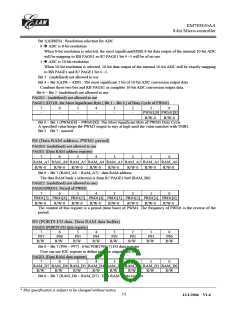
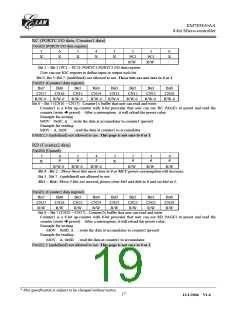
PAGE1,2 : (undefined) not allowed to use
PAGE3 (DT2H: the Most Significant Byte ( Bit 1 ~ Bit 0 ) of Duty Cycle of PWM2)
7
-
6
-
5
-
4
-
3
-
2
-
1
0
PWM2[9] PWM2[8]
R/W-0 R/W-0
Bit 0 ~ Bit 1 (PWM2[8] ~ PWM2[9]): The Most Significant Byte of PWM1 Duty Cycle
A specified value keeps the PWM1 output to stay at high until the value matches with TMR1.
Bit 2 ~ Bit 7 : unused
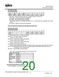
RB (ADC input data buffer)
PAGE0 : (undefined) not allowed to use
PAGE1 (ADC output data register)
7
6
5
4
3
2
1
0
AD7
R
AD6
R
AD5
R
AD4
R
AD3
R
AD2
R
AD1
R
AD0
R
Bit 0 ~ Bit 7 (AD0 ~ AD7) : The last significant 8 bit of 10-bit or whole of 8 bit resolution ADC conversion
output data. Combine there 8 bits and R7 PAGE1 bit4~5 as complete 10-bit ADC conversion output data in 10
bit resolution mode.
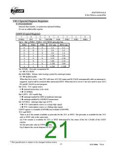
PAGE2 (undefined) not allowed to use. This page is not sure to be 0 or 1
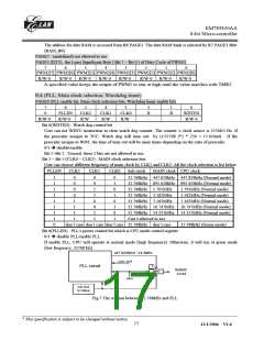
PAGE3 (PRD2: Period of PWM2)
7
6
5
4
3
2
1
0
PRD2[7] PRD2[6] PRD2[5] PRD2[4] PRD2[3] PRD2[2] PRD2[1] PRD2[0]
R/W-0 R/W-0 R/W-0 R/W-0 R/W-0 R/W-0 R/W-0 R/W-0
The content of this register is a period (time base) of PWM2. The frequency of PWM2 is the reverse of the
period.
__________________________________________________________________________________________________________________________________________________________________
* This specification is subject to be changed without notice.
16
12/1/2004 V1.6

 ELAN [ ELAN MICROELECTRONICS CORP ]