EM73962A
4-BIT MICROCONTROLLER
LDL#5h;
LDH #3h;
STDMI #0Ah; RAM[35] ← Ah
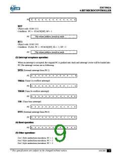
(3) For instruction : SELP, CLPL, TFPL, L regieter be a pointer to indicate the bit of I/O port.
When LR = 0 indicate P4.0
PROGRAM EXAMPLE: To set bit 0 of Port4 to "1"
LDL#00h;
SEPL ; P4.0 ←1
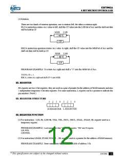
STACK POINTER (SP)
Stack pointer is a 4-bit register which stores the present stack level number.
Before using stack, user must set the SP value first, CPU will not initiate the SP value after reset condition.
When a new subroutine is accepted, the SP will be decreased one automatically, in another word, if
returning from a subroutine, the SP will be increased one.
The data transfer between ACC and SP is by instruction of "LDASP" and "STASP".
DATA POINTER (DP)
Data pointer is a 12-bit register which stores the address of ROM can indicate the ROM code data
specified by user (refer to data ROM).
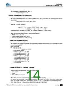
CLOCK AND TIMING GENERATOR
The clock generator is supported by a single clock system, the clock source comes from RC oscillation, the
working frequency range is 480 K Hz to 4 MHz depending on the external resistor.
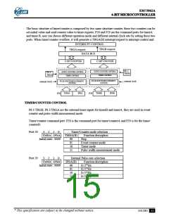
CLOCK AND TIMING GENERATOR STRUCTURE
The clock generator connects outside compoments ( only a resistor connects to VDD and CLK pin).
The clock generator generates a basic system clock "fc".
When CPU sleeping, the clock generator will be stoped until the sleep condition released.
The system clock control generates 4 basic phase signals ( S1, S2, S3, S4 ) and system clock.
sleep
fc
CLK
Clock generator
System clock control
System clock
CLK
RC connection
S1
S2
S3
S4
CLOCK AND TIMING GENERATOR FUNCTION
The frequency of fc is the oscillation frequency for CLK by RC oscillator.
* This specification are subject to be changed without notice.
10.8.2001
13

 ELAN [ ELAN MICROELECTRONICS CORP ]