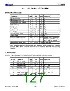
VT82C686B
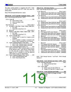
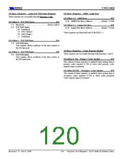
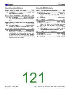
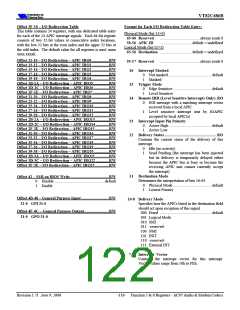
Processor Bus States
FUNCTIONAL DESCRIPTIONS
The VT82C686B supports the complete set of C0 to C3
processor states as specified in the Advanced Configuration
and Power Interface (ACPI) specification (and defined in
ACPI I/O space Registers 10-15):
Power Management
o
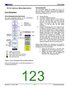
P wer Management Subsystem Overview
C0: Normal Operation
C1: CPU Halt (controlled by software).
The power management function of the VT82C686B is
indicated in the following block diagram:
C2: Stop Clock. Entered when the P_LVL2 register is
read. The STPCLK# signal is asserted to put the
processor in the Stop Grant State. The CPUSTP#
signal is not asserted so that host clocks remain
running.
To exit this state, the chip negates
STPCLK#.
C3: Suspend. Entered when the P_LVL3 register is read.
In addition to STPCLK# assertion as in the C2 state,
the SUSST1# (suspend status 1) signal is asserted to
tell the north bridge to switch to “Suspend DRAM
Refresh” mode based on the 32KHz suspend clock
(SUSCLK) provided by the VT82C686B. If the
HOST_STP bit is enabled, then CPUSTP# is also
asserted to stop clock generation and put the CPU
into Stop Clock State. To exit this state, the chip
negates CPUSTP# and allows time for the processor
PLL to lock. Then the SUSST1# and STPCLK#
signals are negated to resume to normal operation.
During normal operation, two mechanisms are provided to
modulate CPU execution and control power consumption by
throttling the duty cycle of STPCLK#:
a. Setting the THT_EN bit to 1, the duty cycle
defined in THT_DTY (IO space Rx10) is used.
b. THRM# pin assertion enables automatic clock
throttling with duty cycle pre-configured in
THM_DTY (PCI configuration Rx4C).
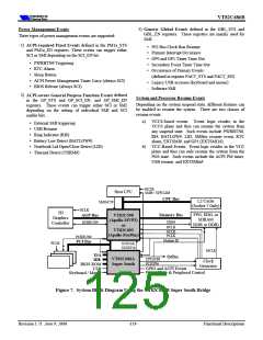
Figure 6. Power Management Subsystem Block Diagram
Refer to ACPI Specification v1.0 and APM specification v1.2
for additional information.
Revision 1.71 June 9, 2000
-117-
Functional Descriptions

 ETC [ ETC ]